Research Facility
Device Fabrication
 Cleanroom
-
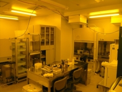

Mainly used for device fabrication of 2D materials. Air shower is equipped.
- Lithography set-up
-
Photolthography set-up for electrode patterning.
Electron Beam Lithography(EBL) set-up with precise piezo motor stage.
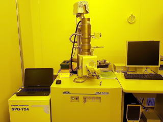
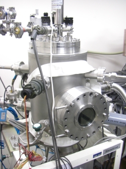
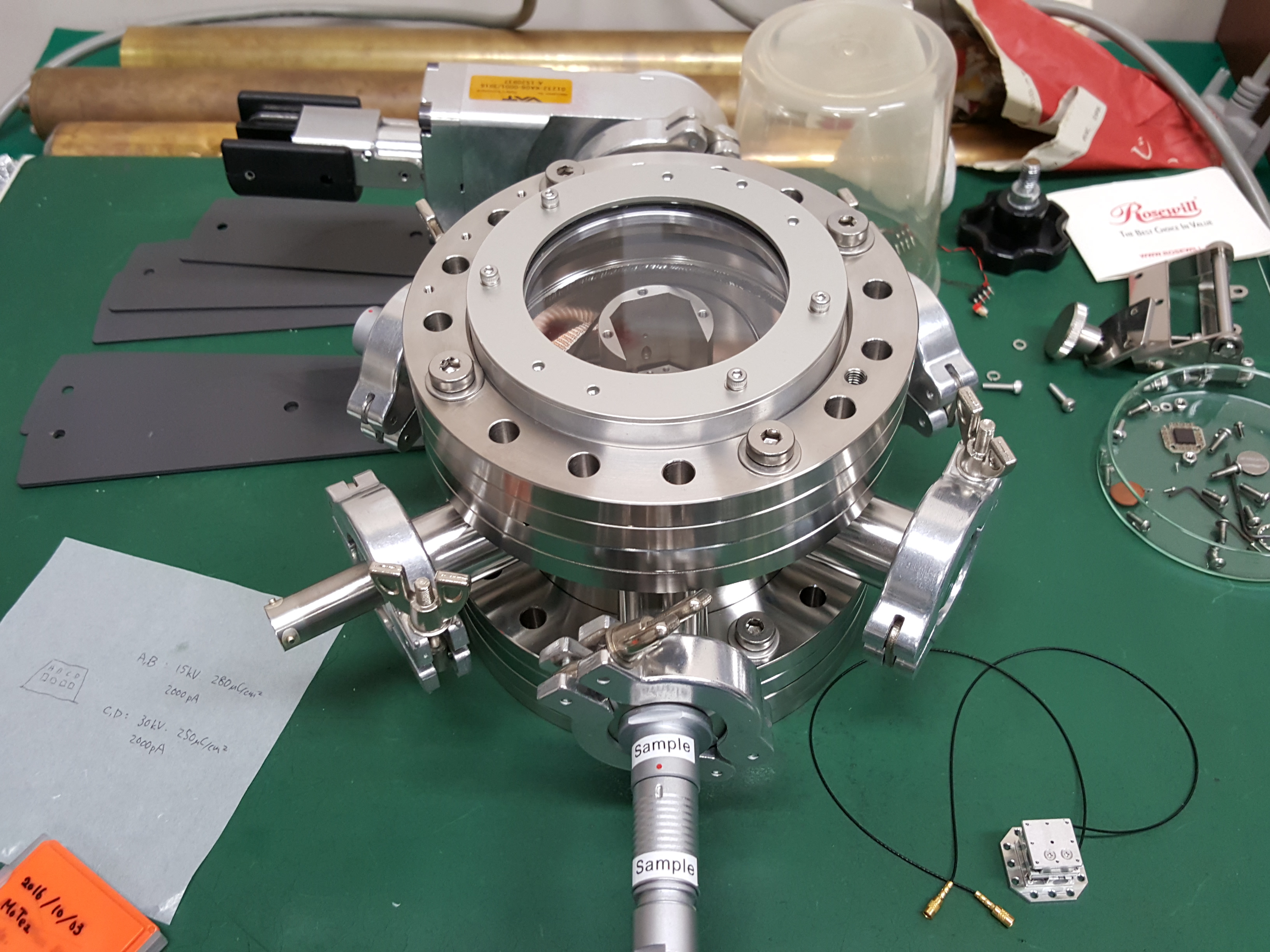
- E-Beam and Thermal Evaporator
-
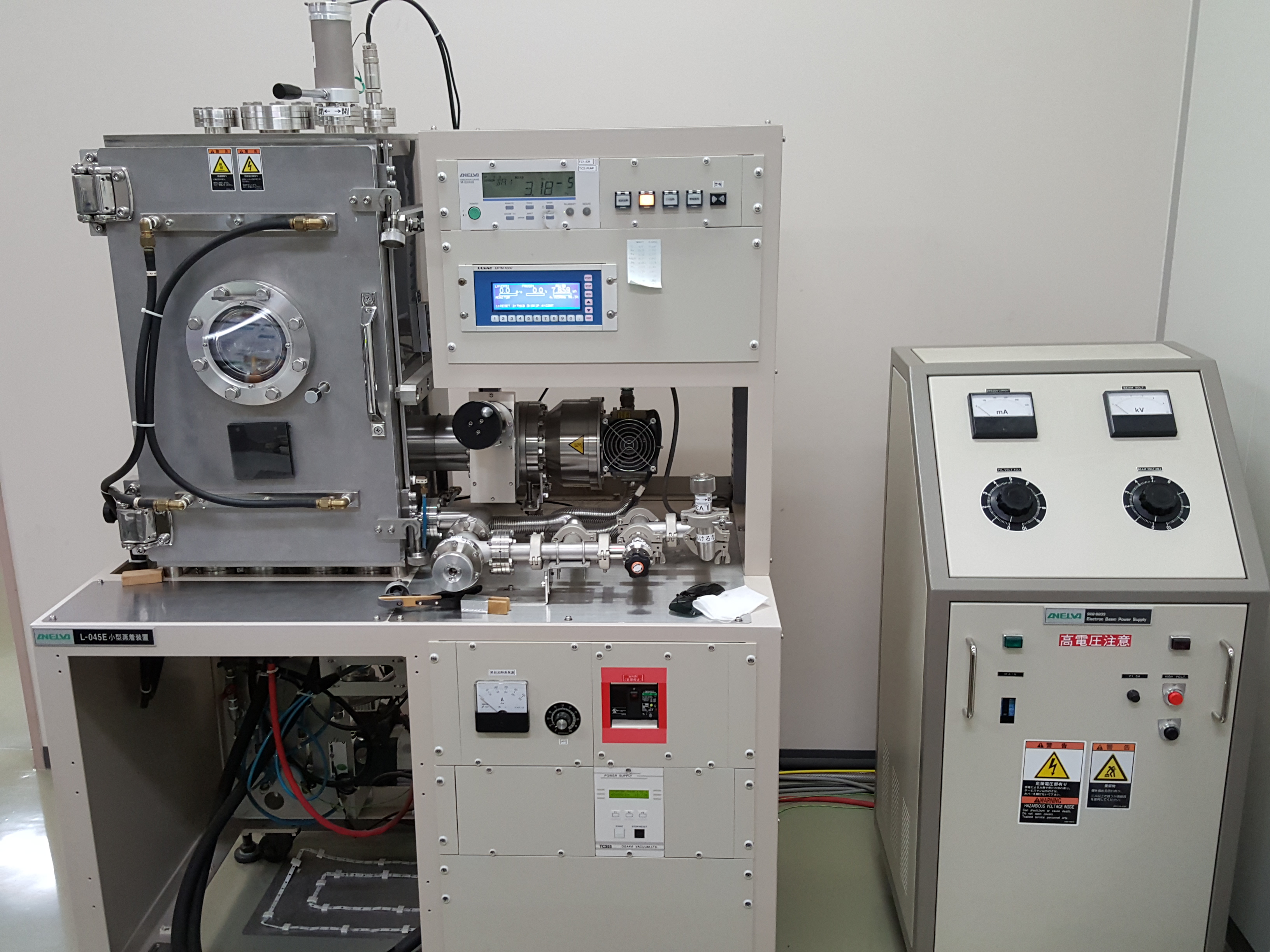
Electron Beam Evaporator under ~10-5Pa base pressure.
Thermal Evaporator for organic materials. By using liquid hellium, available to deposit under liquid He temperature.
More evaporators are avarable.
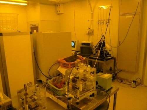
- Other fabrication facility
-
Van der Waals heterostructure factory with optical microscopy.
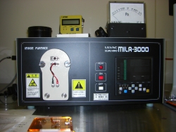
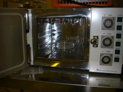
Rapid Thermal Annealer under Ar/H2 environment.
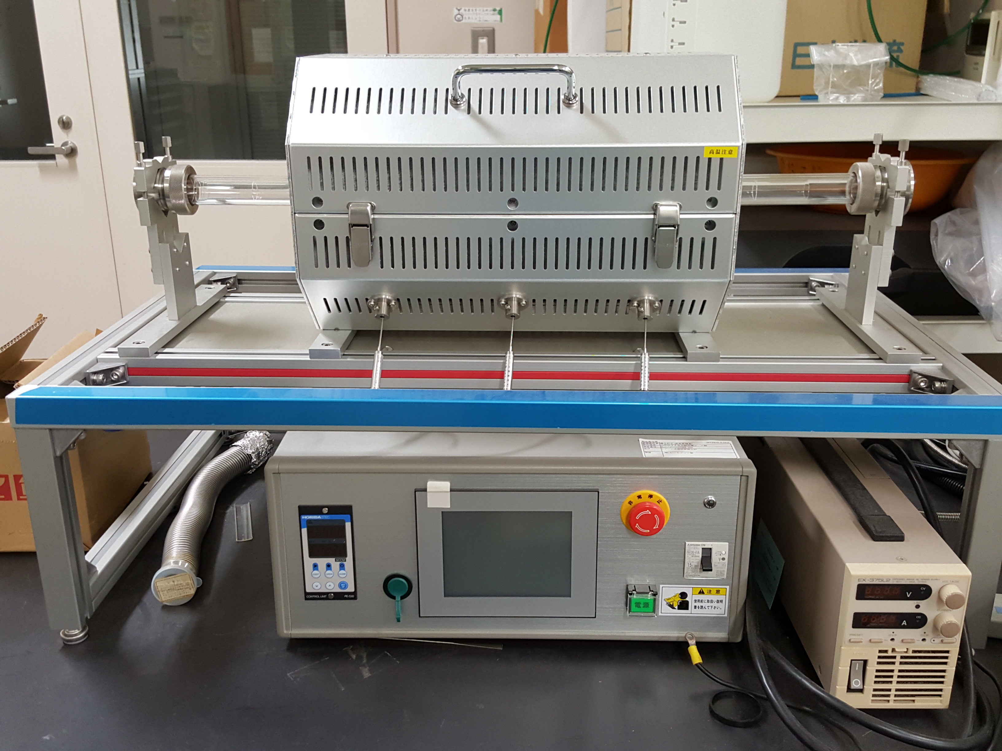
CVT set-up for oxidazation and crystal growth.
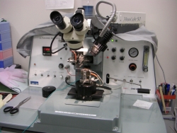
Bondhing machine.
UV ozone cleaner.
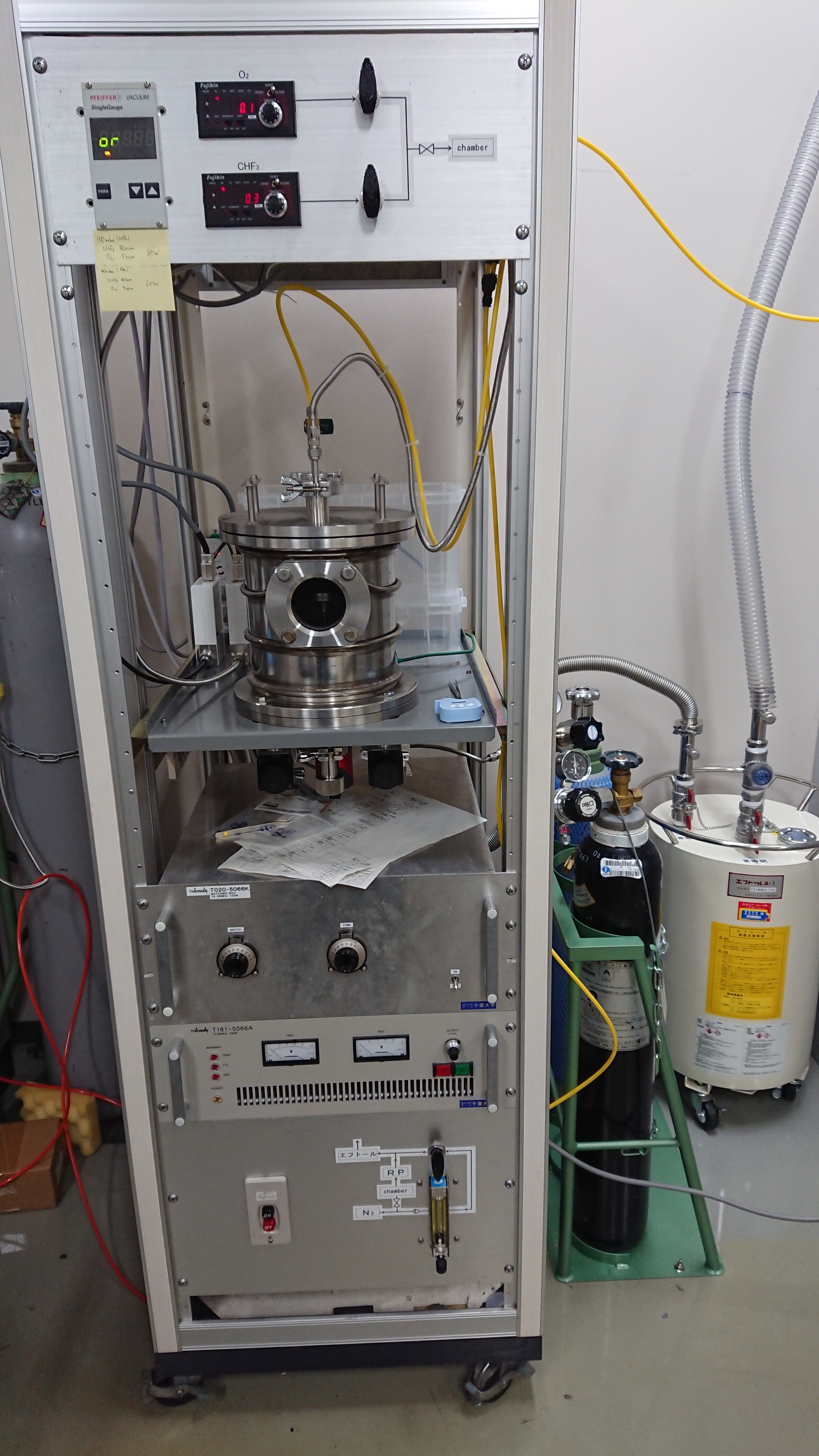
Home-built dry reactive ion etching machine.
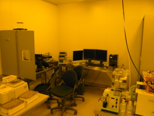
Device Evaluation Facility
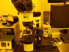
- Probe station
-
Variable temperature probe station. AC/DC transport measurement, optical measurement and high temperature measurement are available.
Variable temperature probe station ranging from 10K to 440K. AC/DC transport measurement is available.
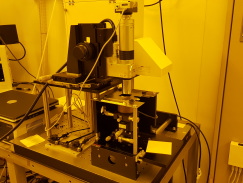
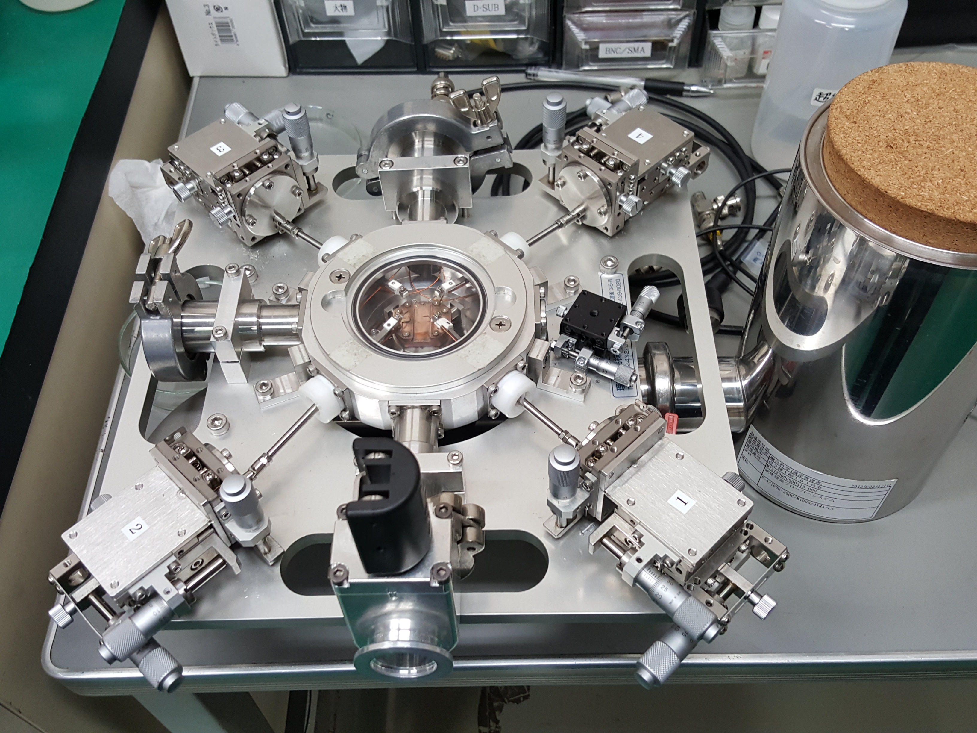
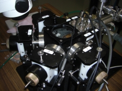
- Scanning probe microscopy
-
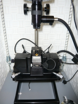
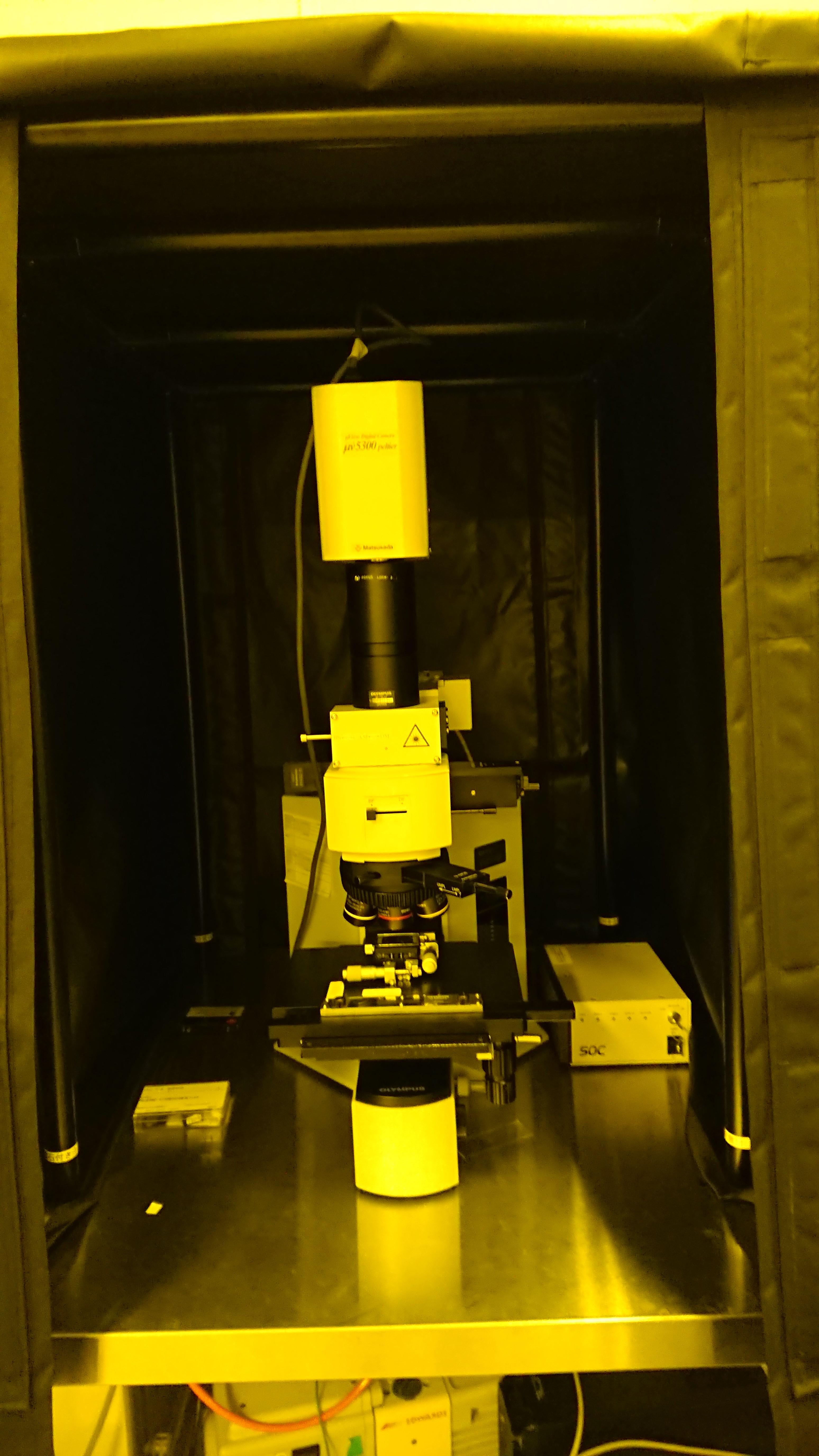
Custormized AFM/EFM/MFM/SGM sysytem. Transport measurement and AFM lithography are also available.
AFM/EFM/SGM sysytem under vacuum.
- Optics
-
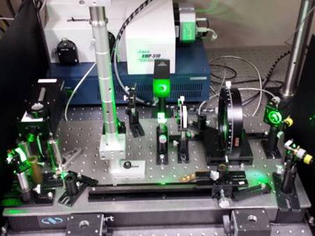
532nm green laser set-up and optical vortex set-up eqquiped with probe station.
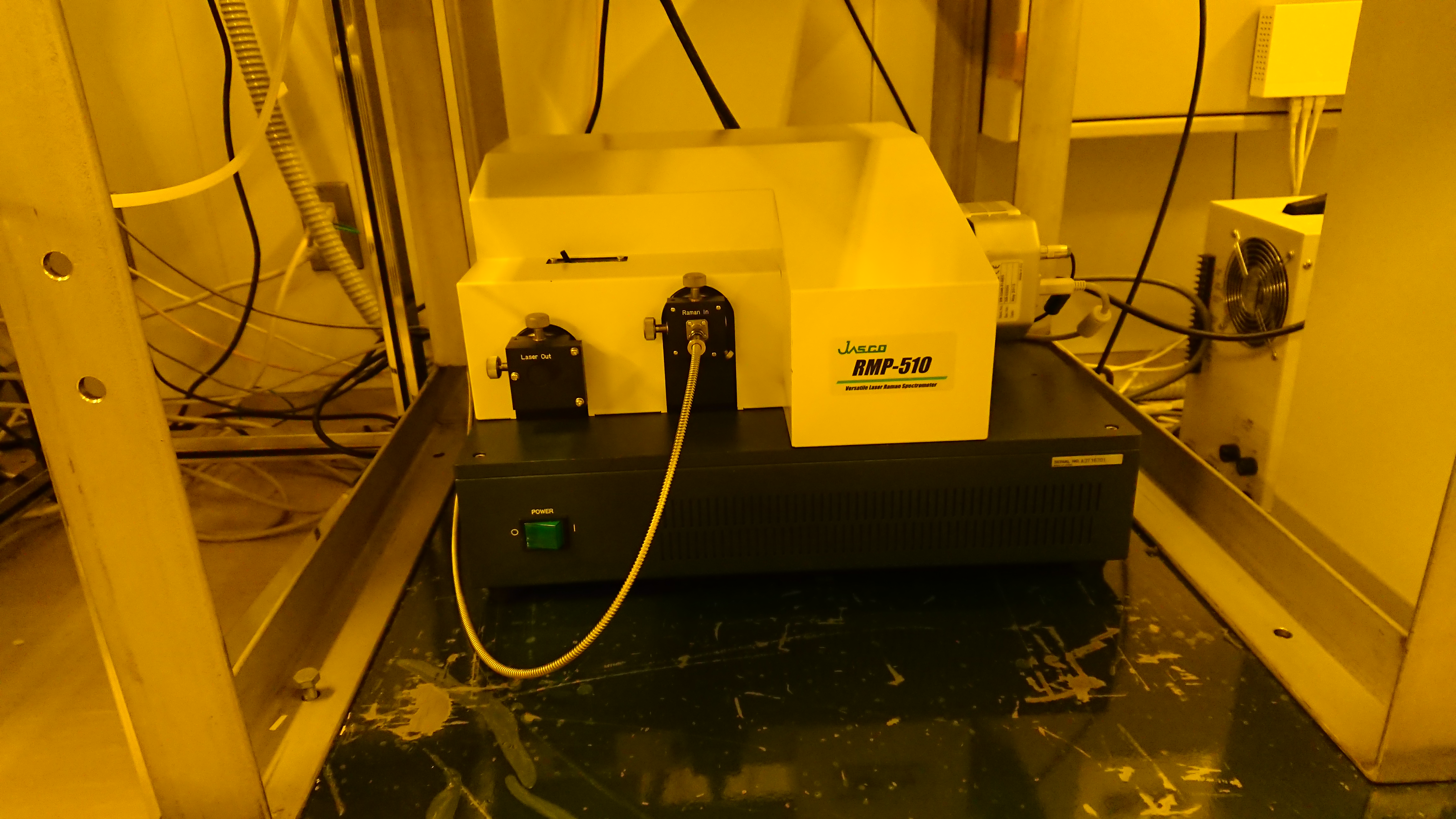
Raman spectroscopy set-up equipped with optical microscope.
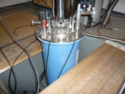
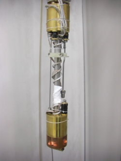
- Low temperature measurement facility
-
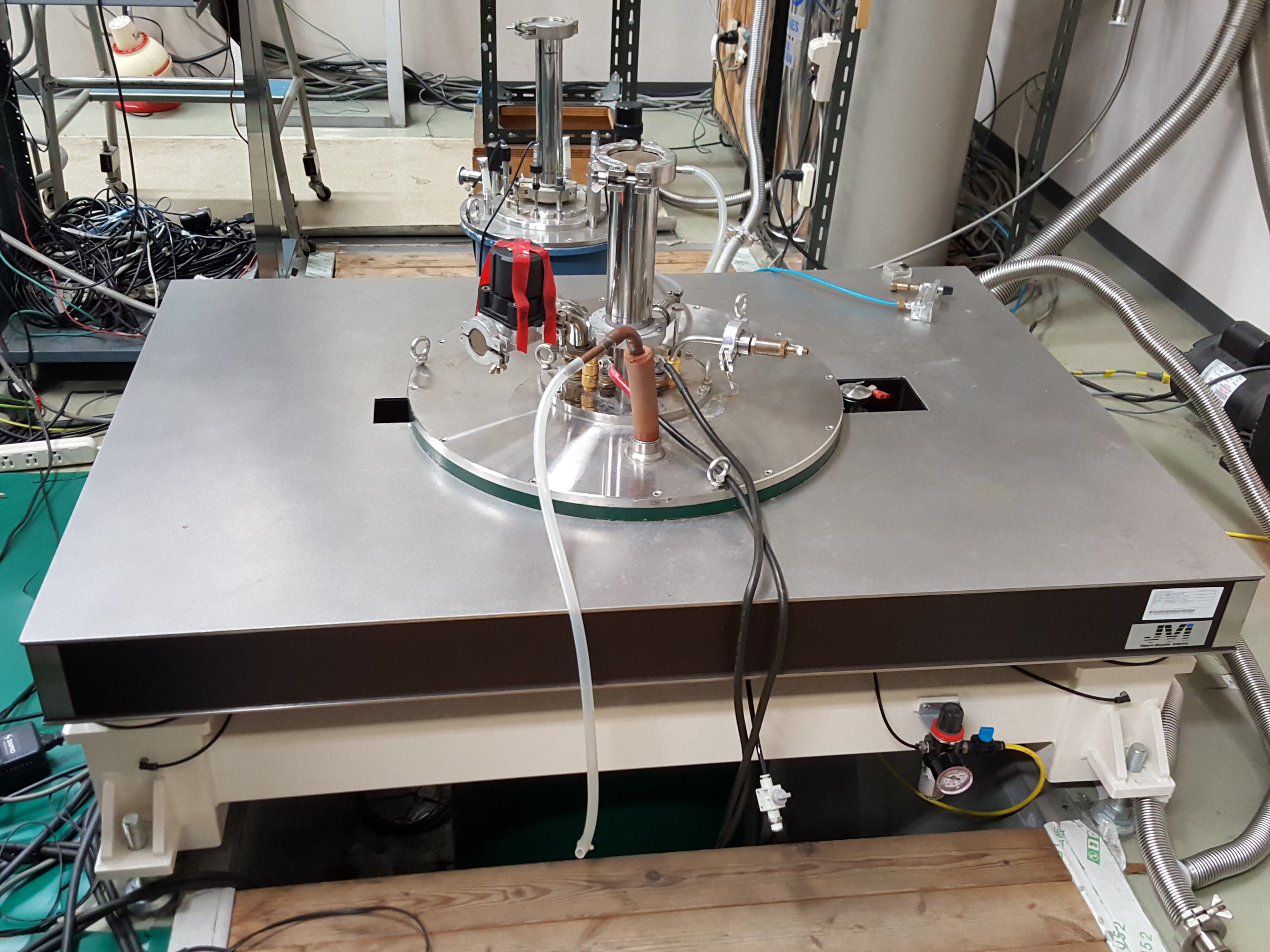
He cryostat with 9 tesla superconducting magnet.
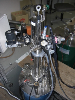
He cryostat with 9 tesla superconducting magnet.
3He insert for 300mK measurement.
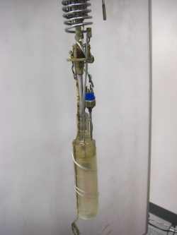
3He/4He dilution insert for 100mK measuremnt.
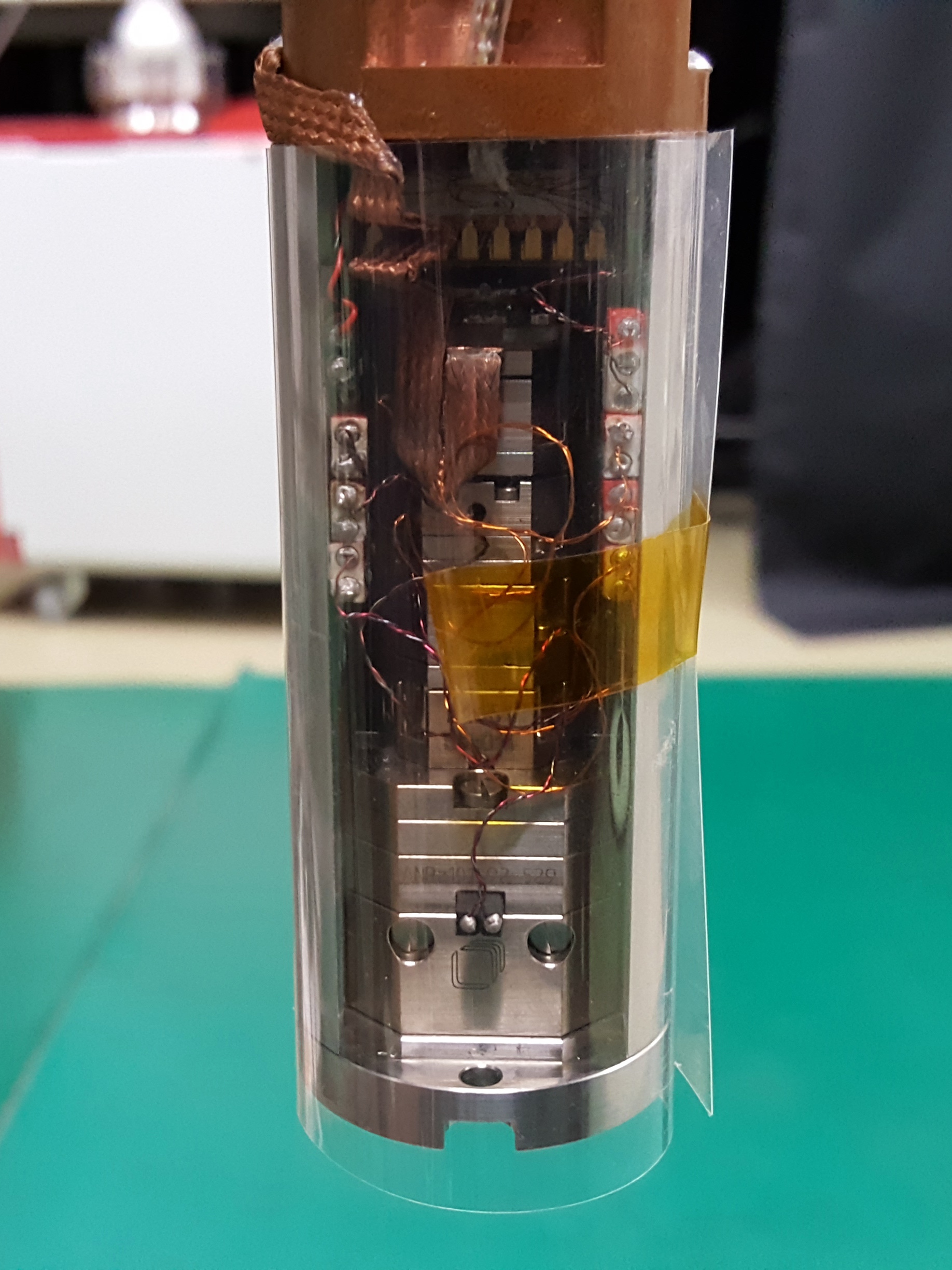
SPM system for ultra low temperature environment. AFM/SGM/EFM measurement is availbale.