Chiba University, Graduate School of Engineering, Department of Materials Science
STM Magnetic and Quantum Spin Imaging Lab. (Toyo Lab.)
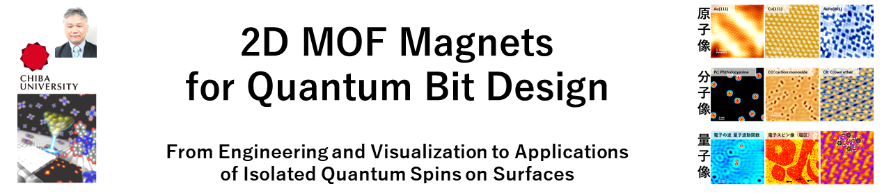
Development of Two-Dimensional Molecular Magnets on Solid Surfaces for Applications in Magnetic and Quantum Spintronics, Molecular Electronics, Solid-State Quantum Sensors, Single-Atom Catalysts, Molecular Machines, and Organic Memristors
|
|
|
|
|
We aim to create, visualize, and utilize isolated quantum spins on solid surfaces. From the atomic and molecular scale, we continue to pursue research that will shape the future quantum society. For those interested in learning more, please refer to the Yamada Laboratory’s press releases and publications.
|

|

|

|

|

|

|
|
|
|
|
|
|
|
|
|

|

|
At Yamada Laboratory, we are tackling the development of mass-producible, ultra-compact organic qubits, a technology essential for the information society of the near future?including AI, robotics, and autonomous vehicles. These qubits can function as high-sensitivity quantum sensors, enabling the detection of faint brain and cardiac signals and even offering potential applications in medical imaging techniques similar to CT scans. Our research focuses on developing organic qubits directly on solid surfaces, which are crucial for device integration. To realize this, we use the smallest magnetic unit of matter, a single atomic spin, as a qubit. Since an isolated atom is inherently unstable and prone to movement, we stabilize and bridge it using flexible yet robust organic molecules. To harness qubits for sensing and information processing, it is essential to achieve initialization, writing, and readout of quantum spin states. Such cutting-edge research requires not only a foundation in quantum mechanics, solid-state physics, and microscopy, but also expertise in microwave technologies?such as those used in smartphone communications?and optical techniques for quantum spin readout. The quantum spin states of our qubits are highly sensitive: when exposed to small molecules such as oxygen, carbon dioxide, or water, charge transfer occurs, altering their properties. In chemistry, such charge-transfer phenomena are known as single-atom catalysis. Moreover, since our qubit research is conducted in ultra-high vacuum and cryogenic environments?conditions close to outer space, our findings hold promise for applications in space exploration. From our previous studies, we discovered that organic qubits are destroyed when placed directly on metals. To address this, we developed a protective membrane. In 2024, we found that organic qubits placed on this membrane, when stimulated by light or voltage, exhibit motion characteristic of a molecular machine. This discovery opens pathways toward novel applications such as drug delivery systems and artificial synapses (neuromorphic devices). To observe and control organic qubits, the Yamada Laboratory has independently developed four scanning tunneling microscopes (STMs) capable of imaging individual atoms. In 2003, we pioneered the world’s first spin-polarized STM (SP-STM) operating at 300 K, which allows not only atomic resolution but also direct observation of the orientation of atomic spins. Currently, we are advancing the development of a unique microscope that combines spin-polarized STM with optically detected magnetic resonance (ODMR), integrating microwave and optical control in a single platform.
| Research Objective |
Please Click!
|
|---|---|
| Research Methodology | UHV-LT-STM, Scanning Tunneling Spectroscopy (STS), Quasi-Particle Interference (QPI) 2D spin band mapping, Spin-Polazied STM Magnetic Imaging, Quantum Spin STM with Microwave and Visible Light Illumination |
| Research Materials | Ultrathin Film Magnet, Nano Magnet, Molecule Magnet, Quantum Magnet, Van der Waals Magnet, NV-center in Diamond, Organic Molecules, 2D COFs, 2D MOFs, Graphene, 2D Magnet, Metal Superconductor, Layered Superconductor |
| Research Fields | Surface Science, Nanomaterials, Surface Magnetism, Spintronics, Quantum Spin, Quantum Magnetism, Organic Molecule, Molecular Machine, Singe-Atom Catalysts, On-Surface Synthesis, Scanning Probe Microscopy, Magnetic Imaging |
Magnets Store Information !
All smartphone information is stored in binary, 1 and 0, using N-S and S-N directions of magnets. The recent information society has been developed through the miniaturization of magnets and devices. The amount of information running worldwide will drastically increase 1000 times in the next decade because of drastic improvements and developments in artificial intelligence (AI), automobiles, and robot technology.
However, the device miniaturization is approaching the limit, which is the smallest material size: atom and molecule. This is called "Moore's law is dead". Another serious aspect that we should pay attention to is the tremendous energy cost of controlling information. One large data center requires operating electric power much larger than the electric power produced by one nuclear plant, which indicates conventional information technology using classical magnets will enhance global warming.
Click here for details of "Data Storage and Magnets"
Are There Any Solutions to Stop Global Warning due to Information Society Development?
 We have studied and developed Advanced Quantum Magnets using Atoms, Molecules, and Quantum Spins. Direct imaging of such the smallest materials is able to be visualized by our home-built Scanning Tunneling Microscopy (STM) setups.
 By the way, What is the Advanced Magnet? The Advanced Magnet consists of magnetic atoms with different magnetic couplings (or interactions) from the classical conventional magnet. Click here for details of [Research Projects]!
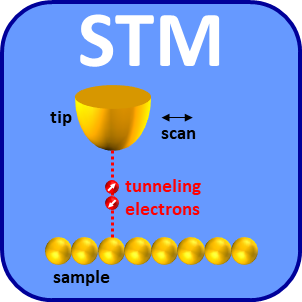
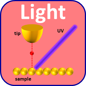
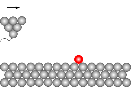
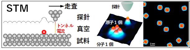
By the way, do you know STM? STM is a microscopy. Although you may imagine optical microscopy, STM does not use light. STM uses an atomically sharp tip probe and images surface morphology (see right Figure). Human eyes also cannot directly detect the surface morphology, but we can feel the morphology by touching fingers on the surface. Similarly, the STM tip scans the surface and detects the morphology, which drastically enhances the space resolution and provides a visualization of the atomic image.
The upper-right Figure shows a model during the STM imaging of an organic molecule (phthalocyanine) adsorbed on an atomic arrangement of the substrate surface. One sphere corresponds to a single atom. Yellow atoms indicate a tip. During the STM imaging, tunneling electrons emit from the apex of the tip like a beam to the sample while the tip does not contact the sample with the separation (No damage to the sample). The tunneling electrons are caused by the quantum effect found by Dr. Einstein. STM detects this tunneling current and scans the surface. [Click here if you want to know STM!]
STM imaging in ultra-high vacuum (<10-8 Pa: extremely low impurity) at cryogenic temperatures (-269 degree Celsius: low thermal energy fluctuation <1 meV) realizes single atom and molecule visualization. [Click here if you want to know our home-built STM setups!]
Movies of our STM setups→ [Movie1] STM course motion と [Movie2] STM light illumination system 。
Especially, STM has the ability to detect a single-atom spin polarization vector (namely, atom magnetic moment = spin angular momentum) by using a spin-polarized magnetic tip.
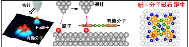
この手法が、スピン偏極走査トンネル顕微鏡(SP-STM)です。「SP-STM」の詳細はこちらをクリック! さらに、STM探針を使うと1個の原子・分子を自在に動かせます。「原子分子マニピュレーション」の詳細はこちらをクリック! この原子が見えるSTMを使って、表面場での新たな低次元磁石の開発を行い、未来の磁気情報媒体・量子ビット材料・光触媒磁気材料・人工知能磁気材料の実現に挑戦しています。「表面合成」の詳細はこちらをクリック!
STM、STS、SP-STMだけでなく、光電子分光、磁気伝導、Kerr磁気計測、原子間力顕微鏡(AFM)、電界放射顕微鏡(FEM)、走査電子顕微鏡(SEM)、化学気相成長装置(CVD)、金属MBE成膜装置、分子昇華装置など、多くの最先端装置を使って研究しています。
山田研の卒業生の進路
90%の学生さんが大学院に進学します。技術職で磁気・情報・計測・IT・半導体メーカーに就職します。さらに博士後期課程ドクター(PhD)を取得して、研究職で企業や教育機関で活躍しています!
【企業】 三菱重工、三菱電機、東芝、キオクシア、リコー、シャープ、村田製作所、セイコーエプソン、富士フィルム(富士ゼロックス)、コニカミノルタ、日本電産、NOK、島津製作所、イビデン、アズビル、キャノンアネルバ、東陽テクニカ、日本証券金融
【アカデミック】 国立研究開発法人物質・材料研究機構 (NIMS), 東京大学大学院、北海道大学大学院、奈良先端科学技術大学院大学、北陸先端大学院大学、総合研究大学院大学、千葉大学大学院
国際共同研究を活発に実施中! 全員、海外留学、継続中!
山田豊和博士は、学習院大学にて博士(理学)を取得後、オランダ・Radbound University NijmegenにてPhDを取得(2005年)しました (ダブルデグリ―)。千葉大学着任前にも、ドイツ・Karlsruhe Institute of TechnologyにてAlexander von Humboldt Research Fellow(2008-2010年)として研究しました。多くの海外の研究者との人脈があります。現在も、台湾・國立清華大学、ドイツ・カールスルーエ工科大学、スペイン・マドリード自治大学との共同研究を中心に、指導学生全員を海外派遣し研究成果を上げています。若手グローバル人材育成に積極的に取り組んでいます。「せまい日本を飛び出し、広い世界を肌で体感し、自分の殻を打ちやぶろう!」
Research Projects
At Yamada Laboratory, we are pursuing the development of organic qubits. By bridging a single atomic spin with organic molecules on a substrate surface, we are creating scalable, ultra-high-density, two-dimensional qubit films using a vacuum epitaxial deposition system. This technology holds promise for diverse applications, including quantum computing, quantum sensing, single-atom catalysis, molecular machines, organic memristors, and artificial synapses.
To realize organic qubits, we are challenging ourselves to “「Create, Visualize, and Utilize” quantum spin centers on solid surfaces.
Project No.1: “Creating” Quantum Spins
The fundamental question tackled at Yamada Laboratory is: “What is a magnet?” Magnets, exemplified by iron, are indispensable in our daily lives. They appear in the motors of cars, trains, and all kinds of moving machinery; in data centers that store the world’s information in the cloud; in headphones; and in power plants that generate electricity. Without magnets, modern life as we know it would be impossible. Japan has long been a world leader in magnet research, for example, the world’s strongest neodymium magnet was developed by Professor Sagawa.
However, for many people, terms such as magnet, magnetization, magnetic field, magnetic flux density, magnetic moment, and angular momentum can be confusing. And when it comes to the “spin” that Yamada Laboratory studies, it may not be immediately clear what it is or where it exists.
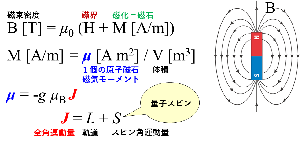 The diagram on the right summarizes these relationships.
Even university students can sometimes find them confusing, but at Yamada Laboratory we consider them fundamental, so we take care to explain them thoroughly.
Mathematically, there are only three key expressions. As shown in high school textbooks, a magnet produces a magnetic flux density, B.
Although invisible to the naked eye, sprinkling iron filings makes the magnetic field lines visible. The greater the number of field lines passing through a unit area, the larger the magnetic flux density.
Stronger magnets have higher flux densities. The unit of magnetic flux density is the tesla (T).
For reference, the Earth’s magnetic field is approximately 0.000046 T, while neodymium magnets available at 100-yen shops typically range from 0.1 to 0.5 T.
The diagram on the right summarizes these relationships.
Even university students can sometimes find them confusing, but at Yamada Laboratory we consider them fundamental, so we take care to explain them thoroughly.
Mathematically, there are only three key expressions. As shown in high school textbooks, a magnet produces a magnetic flux density, B.
Although invisible to the naked eye, sprinkling iron filings makes the magnetic field lines visible. The greater the number of field lines passing through a unit area, the larger the magnetic flux density.
Stronger magnets have higher flux densities. The unit of magnetic flux density is the tesla (T).
For reference, the Earth’s magnetic field is approximately 0.000046 T, while neodymium magnets available at 100-yen shops typically range from 0.1 to 0.5 T.In fact, the magnetic flux density, B, contains both the magnetic field (H) and the magnetization (M). Inside a magnet, there is a magnetization M, while outside the magnet, there is no magnetization?only the magnetic field H. You can think of the magnetization M as representing what we usually imagine a magnet to be. If we multiply this magnetization M by the volume V of the magnet, we obtain the magnetic moment vector of a single atomic magnet (as expressed in the second equation). Suddenly, we are talking about an individual atom?it’s fascinating! This is why, even today, measuring magnetization is a common method to investigate atomic properties.
And now, the third equation. The magnetic moment vector is equal to the product of a coefficient called the g-factor and another coefficient known as the Bohr magneton, giving the total angular momentum vector, J. This total angular momentum is the sum of the orbital angular momentum and the spin angular momentum. Finally, the concept of “spin” emerges. Indeed, this is exactly the “quantum spin” that Yamada Laboratory is developing.
For those who wish to learn more, please refer to the Yamada Laboratory’s press releases and publications. Here, we will provide a brief overview of some aspects of our actual development work.
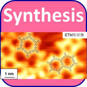
 It is possible to artificially create two-dimensional films on substrate surfaces by combining atoms and molecules (synthesis) with freely designed shapes (i.e., symmetries).
The image on the right is an STM image of a two-dimensional honeycomb lattice successfully developed at Yamada Laboratory in 2024. The film is the world’s thinnest at 0.2 nm, and the hexagonal pores are approximately 2 nm
in diameter. Currently, by bridging a single magnetic atom within each pore using organic molecules, we are advancing the development of two-dimensional honeycomb quantum magnets.
This approach enables the realization of ultra-sensitive quantum sensors, similar to diamond NV quantum sensors, capable of high-precision measurement of various physical quantities, including magnetic fields,
electric fields, and temperature.
By synthesizing organic molecules and magnetic atoms directly on a substrate under vacuum, we can achieve: (1) Diverse design flexibility, (2) Ultra-high-density device fabrication, and (3) Scalability through vacuum epitaxial growth.
To control the structure with such precision, a detailed fundamental understanding of the interactions among magnetic atoms, organic molecules, and the substrate surface is essential.
Moreover, these quantum magnets hold promise for applications as single-atom catalysts and quantum bits.
It is possible to artificially create two-dimensional films on substrate surfaces by combining atoms and molecules (synthesis) with freely designed shapes (i.e., symmetries).
The image on the right is an STM image of a two-dimensional honeycomb lattice successfully developed at Yamada Laboratory in 2024. The film is the world’s thinnest at 0.2 nm, and the hexagonal pores are approximately 2 nm
in diameter. Currently, by bridging a single magnetic atom within each pore using organic molecules, we are advancing the development of two-dimensional honeycomb quantum magnets.
This approach enables the realization of ultra-sensitive quantum sensors, similar to diamond NV quantum sensors, capable of high-precision measurement of various physical quantities, including magnetic fields,
electric fields, and temperature.
By synthesizing organic molecules and magnetic atoms directly on a substrate under vacuum, we can achieve: (1) Diverse design flexibility, (2) Ultra-high-density device fabrication, and (3) Scalability through vacuum epitaxial growth.
To control the structure with such precision, a detailed fundamental understanding of the interactions among magnetic atoms, organic molecules, and the substrate surface is essential.
Moreover, these quantum magnets hold promise for applications as single-atom catalysts and quantum bits.
Project No.1 “Protecting and Controlling” Quantum Spins
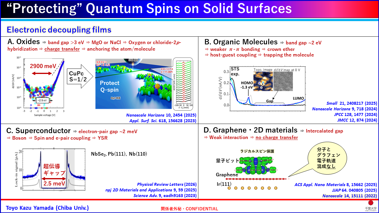
At Yamada Laboratory, in addition to “creating” quantum spins, we have been conducting research on “protecting” and “controlling” quantum spins. Our studies revealed that quantum bits are destroyed when placed directly on a metallic substrate. To protect the quantum spins, we have developed protective layers, technically known as conduction-electron-blocking layers. We have investigated various materials, including MgO oxides, organic molecular films (such as crown ether molecules), superconducting gaps (Nb and NbSe2), graphene, and atomic-layer magnets like Fe2GeTe3 and MnTe. Furthermore, to control quantum spins, we are studying photo-induced reactions and charge transfer caused by adsorption of small molecules, which is related to single-atom catalysis (SAC).
 In 2024, during our development of protective layers for quantum bits, Yamada Laboratory discovered that the molecular magnets used as quantum bits can behave like “molecular machines”,
moving in response to external instructions, much like tiny robots.
In ordinary materials, atoms and molecules adopt energetically stable structures, so there is no natural need for them to change shape or move?they cannot function as “machines.”
To induce motion with an external electrical signal, a specific mechanism is required.
To realize such a “dream molecule,” we focused on crown ether cyclic molecules, which act like convenient pockets capable of incorporating various atoms, molecules, and ions.
The key advantage of crown ether rings is that the ring structure serves as a cavity or pocket, allowing a variety of guest species to be accommodated.
By combining this ring with ferrocene molecules capable of electrically controlled rotational motion, we were able to create a functional molecular machine (see video on the right).
Initially, these ferrocene molecules contained Fe ions, making them suitable candidates for quantum bits.
Remarkably, the size of these molecular machines is only about 1 nm (1 nanometer = 10^{-9} meters), making them the world’s smallest molecular machines.
This groundbreaking discovery was achieved through the following procedure. Ferrocene molecules consist of an Fe ion at the center, flanked above and below by five-membered rings,
giving the molecule a drum-like shape. The unique feature is that when the Fe ion undergoes a valence change (Fe2+ <-> Fe3+), the two five-membered rings rotate by approximately 36 degrees.
If the valence of the Fe ion can be controlled by an external electrical signal, this rotational motion can be converted into mechanical rotation of the molecule.
However, when ferrocene molecules are adsorbed directly onto a substrate surface, particularly on noble metals, they are quickly destroyed.
This had been a major obstacle to fabricating thin-film devices using ferrocene molecules. To improve durability and fix the ferrocene molecules on the substrate, we attached ammonium salts to the ferrocene molecules.
This modified molecule is referred to as ferrocene ammonium salt (Fc-amm). When these molecules are adsorbed onto crown ether cyclic molecules arranged regularly on the substrate,
the crown ether rings effectively capture the ammonium salts, allowing ferrocene molecules to be adsorbed on the solid surface without being destroyed, a world-first achievement.
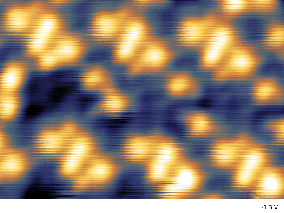
Next, an STM tip was positioned above the ferrocene molecule, and a voltage of -1.3 V was applied. Holes from the tip entered the molecular orbital of the ferrocene, converting Fe2+ <-> Fe3+.
This caused the five-membered rings of the ferrocene to rotate like a car tire, resulting in lateral motion of the molecule. There are two orientations: face-on and edge-on. Only the edge-on orientation,
lying horizontally, exhibited lateral motion, enabling voltage-controlled operation of the molecular machine, as seen in the video.
A fundamental understanding of the molecular system is essential for controlling the molecular machine.
In 2024, during our development of protective layers for quantum bits, Yamada Laboratory discovered that the molecular magnets used as quantum bits can behave like “molecular machines”,
moving in response to external instructions, much like tiny robots.
In ordinary materials, atoms and molecules adopt energetically stable structures, so there is no natural need for them to change shape or move?they cannot function as “machines.”
To induce motion with an external electrical signal, a specific mechanism is required.
To realize such a “dream molecule,” we focused on crown ether cyclic molecules, which act like convenient pockets capable of incorporating various atoms, molecules, and ions.
The key advantage of crown ether rings is that the ring structure serves as a cavity or pocket, allowing a variety of guest species to be accommodated.
By combining this ring with ferrocene molecules capable of electrically controlled rotational motion, we were able to create a functional molecular machine (see video on the right).
Initially, these ferrocene molecules contained Fe ions, making them suitable candidates for quantum bits.
Remarkably, the size of these molecular machines is only about 1 nm (1 nanometer = 10^{-9} meters), making them the world’s smallest molecular machines.
This groundbreaking discovery was achieved through the following procedure. Ferrocene molecules consist of an Fe ion at the center, flanked above and below by five-membered rings,
giving the molecule a drum-like shape. The unique feature is that when the Fe ion undergoes a valence change (Fe2+ <-> Fe3+), the two five-membered rings rotate by approximately 36 degrees.
If the valence of the Fe ion can be controlled by an external electrical signal, this rotational motion can be converted into mechanical rotation of the molecule.
However, when ferrocene molecules are adsorbed directly onto a substrate surface, particularly on noble metals, they are quickly destroyed.
This had been a major obstacle to fabricating thin-film devices using ferrocene molecules. To improve durability and fix the ferrocene molecules on the substrate, we attached ammonium salts to the ferrocene molecules.
This modified molecule is referred to as ferrocene ammonium salt (Fc-amm). When these molecules are adsorbed onto crown ether cyclic molecules arranged regularly on the substrate,
the crown ether rings effectively capture the ammonium salts, allowing ferrocene molecules to be adsorbed on the solid surface without being destroyed, a world-first achievement.
Next, an STM tip was positioned above the ferrocene molecule, and a voltage of -1.3 V was applied. Holes from the tip entered the molecular orbital of the ferrocene, converting Fe2+ <-> Fe3+.
This caused the five-membered rings of the ferrocene to rotate like a car tire, resulting in lateral motion of the molecule. There are two orientations: face-on and edge-on. Only the edge-on orientation,
lying horizontally, exhibited lateral motion, enabling voltage-controlled operation of the molecular machine, as seen in the video.
A fundamental understanding of the molecular system is essential for controlling the molecular machine.
Project No.2 “Visualizing” Quantum Spins
One academic approach to the question “What is a magnet?” is to “observe a magnet”. As explained at the beginning of this website, the orientation of a magnet’s N and S poles cannot be seen with the naked eye. When observing a magnet, it is also crucial to consider which property you want to measure: magnetic flux density, magnetic field, magnetization, magnetic moment, or spin angular momentum. At Yamada Laboratory, our goal is to “visualize quantum spins”.
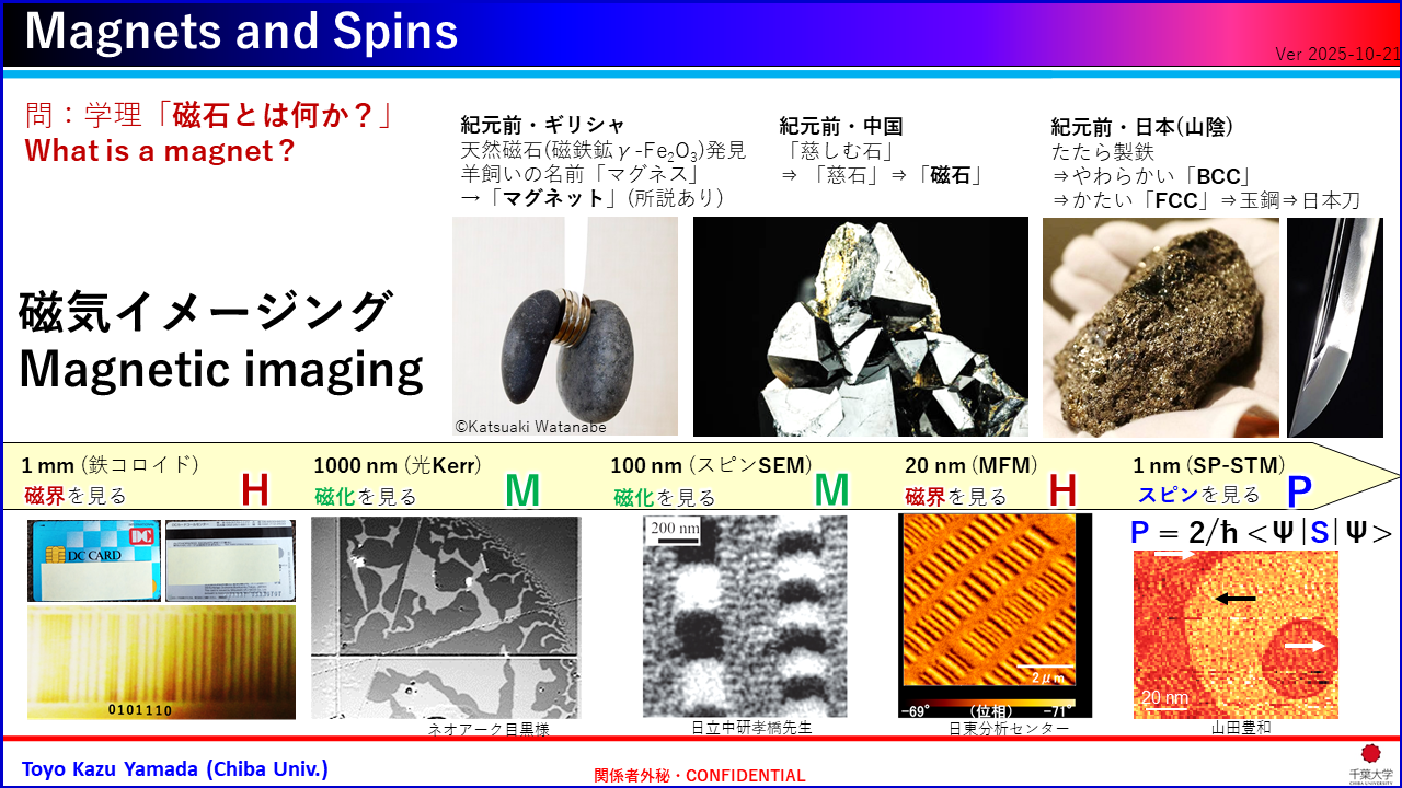 Please refer to the figure. Throughout history, humans have developed various techniques to observe magnets, commonly referred to as “magnetic imaging.”
Why “magnetic”? The simplest method is to sprinkle iron filings around a magnet. The filings align along the magnet’s field lines, accumulating near the N pole but not the S pole.
Using this approach, one can even observe the orientation of a credit card magnet, representing information as 1s and 0s. However, the resolution is limited to what the naked eye can see.
Importantly, what is being visualized here is not the magnet itself, but the magnetic field produced by the magnet.
By using the optical Kerr effect, we can employ a light microscope to observe magnets as small as ~1000 nm. Since light interacts with the magnetization of the magnet, what the Kerr microscope actually observes is magnetization.
For even smaller magnets, a scanning electron microscope (SEM) can visualize features around 100 nm?comparable in size to the coronavirus. In this case, the spin-SEM is also detecting magnetization.
A further step in resolution is achieved with the magnetic force microscope (MFM), which can observe magnets as small as ~20 nm, similar in size to those used in modern data centers.
However, the MFM does not observe the magnet itself, but rather the magnetic field.
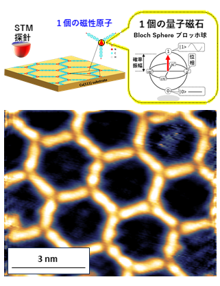
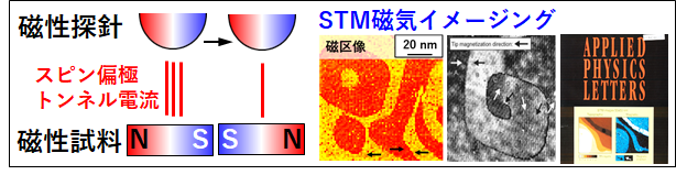
As you may have noticed, there are very few microscopes capable of directly observing “quantum spins.” To address this, Yamada Laboratory pioneered the development of the spin-polarized scanning tunneling microscope (SP-STM) in 2003, which can directly visualize quantum spins.
Even today, only about 30 locations worldwide have successfully used this cutting-edge technology.
Thanks to SP-STM, it is now possible to observe the tiny quantum spins of individual atoms and molecules.
Since 2024, we have been integrating machine learning with SP-STM to detect previously unseen quantum spin information that is invisible to the human eye.
Please refer to the figure. Throughout history, humans have developed various techniques to observe magnets, commonly referred to as “magnetic imaging.”
Why “magnetic”? The simplest method is to sprinkle iron filings around a magnet. The filings align along the magnet’s field lines, accumulating near the N pole but not the S pole.
Using this approach, one can even observe the orientation of a credit card magnet, representing information as 1s and 0s. However, the resolution is limited to what the naked eye can see.
Importantly, what is being visualized here is not the magnet itself, but the magnetic field produced by the magnet.
By using the optical Kerr effect, we can employ a light microscope to observe magnets as small as ~1000 nm. Since light interacts with the magnetization of the magnet, what the Kerr microscope actually observes is magnetization.
For even smaller magnets, a scanning electron microscope (SEM) can visualize features around 100 nm?comparable in size to the coronavirus. In this case, the spin-SEM is also detecting magnetization.
A further step in resolution is achieved with the magnetic force microscope (MFM), which can observe magnets as small as ~20 nm, similar in size to those used in modern data centers.
However, the MFM does not observe the magnet itself, but rather the magnetic field.
As you may have noticed, there are very few microscopes capable of directly observing “quantum spins.” To address this, Yamada Laboratory pioneered the development of the spin-polarized scanning tunneling microscope (SP-STM) in 2003, which can directly visualize quantum spins.
Even today, only about 30 locations worldwide have successfully used this cutting-edge technology.
Thanks to SP-STM, it is now possible to observe the tiny quantum spins of individual atoms and molecules.
Since 2024, we have been integrating machine learning with SP-STM to detect previously unseen quantum spin information that is invisible to the human eye.
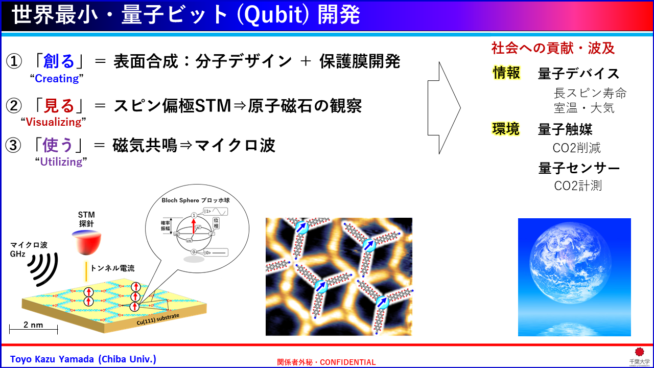
Project No.3 “Utilizing” Quantum Spins
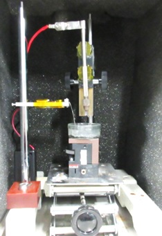
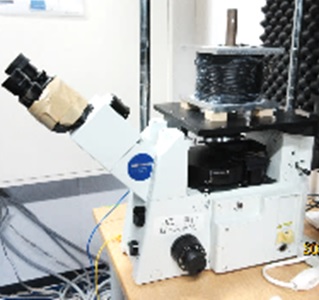
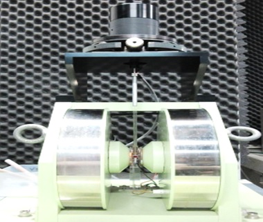
The final step after “creating” and “visualizing” quantum spins is “utilizing” them. Once atomic magnets are bridged with organic molecules on a solid surface, it becomes crucial to harness the quantum spins contained within these atomic magnets. To achieve this, we are introducing novel magnetic resonance techniques into the systems we have developed so far, including the spin-polarized scanning tunneling microscope (SP-STM), and experimental environments that replicate outer space conditions, such as ultra-high vacuum and extreme cryogenic temperatures. The figure below shows the conventional quantum microscopes developed in our laboratory up to 2024.
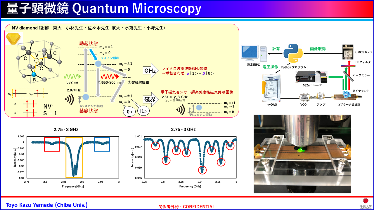 We conducted preliminary experiments in air using a standard optical microscope. Visible light (532 nm) was irradiated from the objective lens onto the sample.
The sample contained nitrogen-vacancy (NV) centers in diamond with electron spin angular momentum S = 1 (triplet) and zero-field splitting. Microwave signals were generated by an oscillator, amplified,
and delivered to the diamond via a coplanar waveguide. The microwaves excite electron spins from the ground state |0> to the excited state |1>.
These excited electron spins are further optically excited by visible light. When the electron is excited from the ground state, it fluoresces and returns to the ground state.
However, if it is excited from the |1> state, it returns to the ground state via a non-radiative pathway, resulting in a decrease in fluorescence intensity only when magnetic resonance occurs.
A long-pass filter was placed in front of the CCD camera on the optical microscope to selectively detect fluorescence. By scanning the microwave frequency applied to the diamond, a dip in fluorescence is observed,
as shown in the figure. When an external magnetic field is applied, the degeneracy of the |1> orbital is lifted (Zeeman splitting), producing multiple dips.
In this way, by combining visible light & fluorescence with microwave excitation, it is possible to observe the quantum spin states of NV centers in diamond.
We conducted preliminary experiments in air using a standard optical microscope. Visible light (532 nm) was irradiated from the objective lens onto the sample.
The sample contained nitrogen-vacancy (NV) centers in diamond with electron spin angular momentum S = 1 (triplet) and zero-field splitting. Microwave signals were generated by an oscillator, amplified,
and delivered to the diamond via a coplanar waveguide. The microwaves excite electron spins from the ground state |0> to the excited state |1>.
These excited electron spins are further optically excited by visible light. When the electron is excited from the ground state, it fluoresces and returns to the ground state.
However, if it is excited from the |1> state, it returns to the ground state via a non-radiative pathway, resulting in a decrease in fluorescence intensity only when magnetic resonance occurs.
A long-pass filter was placed in front of the CCD camera on the optical microscope to selectively detect fluorescence. By scanning the microwave frequency applied to the diamond, a dip in fluorescence is observed,
as shown in the figure. When an external magnetic field is applied, the degeneracy of the |1> orbital is lifted (Zeeman splitting), producing multiple dips.
In this way, by combining visible light & fluorescence with microwave excitation, it is possible to observe the quantum spin states of NV centers in diamond.
At Yamada Laboratory, we have integrated optically detected magnetic resonance (ODMR) into the SP-STM under ultra-high vacuum and extreme cryogenic conditions, creating a truly one-of-a-kind microscope. Furthermore, to control quantum spins and enable their operation as quantum bits, pulsed excitation is required. We are currently implementing nanosecond pulses to achieve precise quantum spin state control.
「磁石」とは何か?
「磁石」とは何か?これは極めて難しい「問い」です。
人類は元素表の中の「鉄(Fe)、コバルト(Co)、ニッケル(Ni)」が磁石であることを発見しました。 強い磁石を作るには、元素表の中の、鉄(Fe)、コバルト(Co)、ニッケル(Ni)の三つの元素が必ず入っていなくては作れません。世界最強サマコバ(SmCo)磁石やネオジム(NbFeB)磁石もCoやFeを含んでいます。じつは元素表の真ん中にあたりにある、3d遷移金属(Sc, Ti, V, Cr, Mn, Fe, Co, Ni, Cu, Zn)、4f希土類金属(通称レアメタル La, Ce, Pr, Nd, Pm, Sm, Eu, Gd, Tb, Dy, Ho, Er, Tm)、も磁石になります。
磁石は1個の原子になっても磁石です。さらに人類は、原子の原子核を取り巻く電子軌道の内、最外殻に3d軌道と4f軌道を持つ元素だけが「磁石」になることを発見しました。3d軌道と4f軌道だけでフント則が成り立つことも発見しました。しかし、なぜ、神様が3d軌道と4f軌道だけにフント則を与えたのか分かりません。
もうひとつ不思議なことがあります。最外殻に3d軌道を持つ元素は12個あります。K (3d04s1)、Ca (3d04s2)、Sc (3d14s2)、Ti (3d24s2)、V (3d34s2)、Cr (3d54s1)、Mn (3d54s2)、Fe (3d64s2)、Co (3d74s2)、Ni (3d84s2)、Cu (3d104s1)、Zn (3d104s2)、です。しかし、Fe、Co、Niだけが強い磁石、強磁性磁石、になります。なぜでしょうか?
これは、原子と原子の間の「磁気結合(J)」が大切な役割を示します。 皆さんも手で磁石をもって磁石と磁石を近づけた際、N極とN極が反発したり、N極とS極が引きつけあう力を感じたことがあると思います。1個の原子になっても磁石ですので、同じような力が働きます。これが磁気結合(J)です。二つの磁石の間の磁気結合が平行な時はJ = +1、反平行な時は J = -1です。実は、Fe、Co、Niだけ磁気結合が平行 (J = +1)なのです。しかし、元素表でFeのすぐ隣のMnは磁気結合が反平行 (J = -1)であるため、隣り合う原子の磁石同士で漏れ出る磁束が収束するため強い磁石になりません。反強磁性磁石と呼ばれます。しかし、なぜ物質によって磁気結合が大きく変わるのか分かっていません。
しかし、面白いことに完全には理解できていない磁気結合が、現在の情報社会を支えています。ハードディスクドライブ(HDD)内で磁石の向きを読み取る磁気抵抗センサは、強磁性膜と反強磁性膜の間の磁気結合を利用しています。
右図をご覧ください。
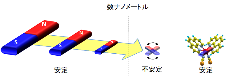
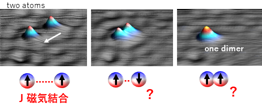 1個のFe原子を、もう一個のFe原子に近づけていきます。磁気結合はどうなるのでしょうか?遠く離れていれば磁気結合は弱く、近づくと強まるように思えます。しかし、実際の磁気結合はそんなに単純ではありません。右図の場合は、Fe原子はCu基板表面にいます。Cu表面には4s電子が自由に動き回っています。そのため、RKKY相互作用が磁気結合に働き、磁気結合は距離によって波打つように変化するのです。考えかたによっては、原子と原子の距離を制御できれば磁気気結合が制御できることを示唆します。つまり、磁性原子間の磁気結合を制御することで、新たな磁石が開発できるのです。
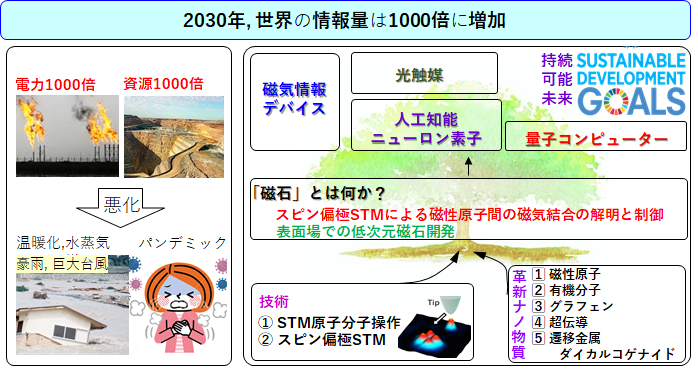
山田ラボでは、未来の情報社会を実現し地球環境問題を解決するため、磁性原子間の磁気結合の解明と制御に挑戦しています(下図)。自動運転車・ロボット開発など今後も情報社会は発展します。2030代、世界の情報量は現在の1021個から1024個に増えます。既存の材料・技術のままであれば単純に1000倍の電力・資源が必要です。現在のデータセンター消費電力量は、原子力発電所1基の発電量を上回ります。そのため、情報社会発展は、地球温暖化に拍車をかけます。大量の水蒸気は多くの水害を生み、さらなる資源開発は未知のウィルスやパンデミックの原因となります。
そのため、既存の磁石に代わる「新たな磁石」が必要です。新たな磁石を使い、未来の磁気情報デバイス・量子コンピューター・光触媒・人工知能の実現に貢献します(下図)。
では、どのようにすれば、自然界の磁石の原子間距離を変えることができるのでしょうか?
「案1」電界や圧力をかけて、無理やり距離を変える!?
「案2」有機分子や酸化物のなかに磁石の原子を閉じ込めて距離をかえる?
「案3」原子レベルで鋭い針をつかって、基板表面の磁石の原子をつついて動かして距離をかえる!?
上の三つのどの案も「本当にそんなことができるの?」と思うような方法ですね。でも、本当に現在の科学の力では上記の三つが可能です!山田ラボでは、この三つの手法を使って、新たな磁石の研究開発を行っています。
我々の研究では、「磁性原子」間を「有機分子」で架橋すると磁気結合はどのように変化するのか?原子と原子の間の磁気結合は、多様な表面場である「金属」「酸化物」「グラフェン」「原子層物質」「超伝導」で変化するのか?磁性膜の間の磁気結合は、スペーサー層の種類(金属、酸化物、グラフェン、原子層物質、超伝導でどう変化するのか?解明に取り組み、新たな磁石開発を実施しています。
さらに、、多様な表面場での(光)化学反応を用いた新たな低次元磁性体の開発を実施中です。表面場ではSTM観察しながら「合成プロセスの見える化」が可能です。光や熱によるミクロな化学反応を観察する事で新たな知見が得られます。特に、表面場で作製した分子原子格子は金属有機構造体(MOF)になります。MOFは多孔質材料のため、水素や二酸化炭素の貯蔵が可能です。磁性原子を混ぜて紫外光を照射する事で「光触媒」が生じ、二酸化炭素の分解が可能です。
【1】マスコミ報道 (NHK, 読売新聞, 朝日新聞, 千葉日報, 他)
記者の皆様に、山田ラボの研究を分かりやすくご説明いただいております。ぜひご覧ください。
 NHK news |
毎日新聞、朝日新聞、千葉日報、日本経済新聞 |
読売新聞、毎日新聞、千葉日報 |
日本経済新聞, 千葉日報1面, 日刊工業新聞, 日経産業新聞, 産業新聞 |
日刊産業新聞, WEBリリース |
読売新聞、毎日新聞、千葉日報 |
2026-2-26
【Press Release】論文はこちら!
鉛のもつ二つの超電導相を原子の積み重ねのずれで制御! ~超伝導内の積層欠陥がもたらす効果の可視化に成功~2次元薄膜で1次元電子ストライプ構造を創る!
Press release: Japanese version Download, PDF.
【HP】
【PR TIMES】
【X】
【Facebook】
毎日新聞
2025-9-26
【Press Release】論文はこちら!
2次元薄膜で1次元電子ストライプ構造を創る!
~鉄磁石とマンガン磁石の界面磁気フラストレーションを活用~
Press release: Japanese version Download, PDF.
【HP】
【PR TIMES】
【X】
【Facebook】
日本経済新聞, EE Times Japan Nikkei Tech Foresight (日経テックフォアサイト)
2025-8-7
【Press Release】論文はこちら!
磁石の表面上で孤立した量子スピンの作製に成功
~磁気トンネル接合MgO/Feを用いた量子ビット開発へ~
 Press release: Japanese version
Download, PDF.
Press release: Japanese version
Download, PDF.
【PR TIMES】
【大学HP】
【X】
【Facebook】
日本経済新聞, 時事通信
Press release: English version Download, PDF.
 【EurekAlert英】
【EurekAlert日】
【CHIBADAI NEXT】
【大学HP】
【LinkedIn】
【Facebook】
2025-7-24
【Press Release】論文はこちら!
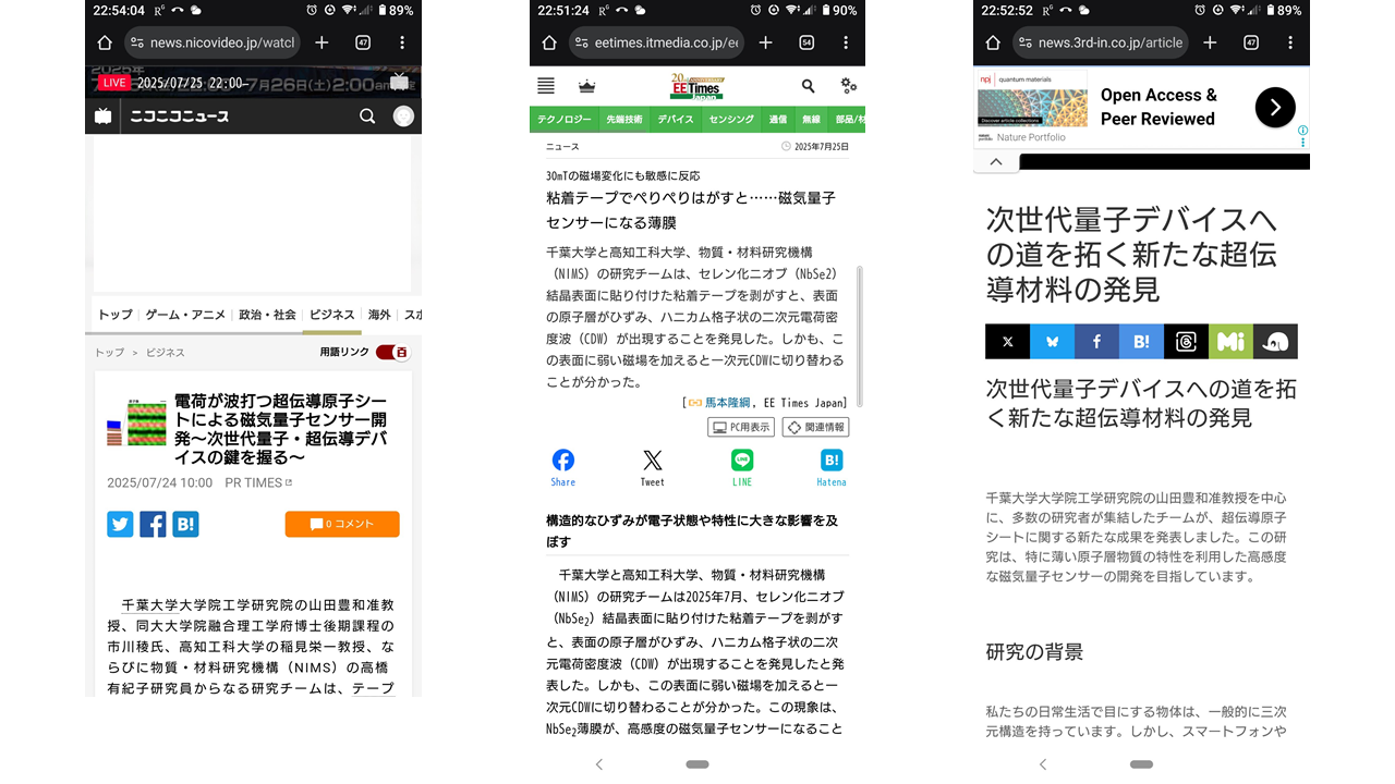
電荷が波打つ超伝導原子シートによる磁気量子センサー開発
~次世代量子・超伝導デバイスの鍵を握る~
 Press release: Japanese version
Download, PDF.
Press release: Japanese version
Download, PDF.
【PR TIMES】
【大学HP】
【X】
Online News
日本経済新聞, 千葉日報
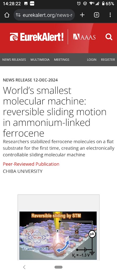
2024-12-12
【Press Release】論文はこちら!
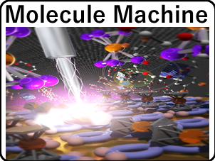
フェロセン分子の「世界最小・分子マシン」機能を発見 !
~新たな触媒・分子エレクトロニクス・量子材料の開発へ~
Press release: Japanese version Download, PDF.
Press release: English version Download, PDF.
千葉大学大学院工学研究院の山田豊和准教授、ピータークリューガー教授の研究グループ、分子科学研究所の解良聡教授、台湾國立清華大学の堀江正樹教授の研究グループから成る国際共同研究チームは、世界で初めて、固体表面上でフェロセン分子を壊すことなく固定できることを実証しました。この発見は、走査トンネル顕微鏡(STM)装置を用いた表面観測により、様々な原子・分子・イオンを取り込むことのできる「クラウンエーテル環状分子」と、有機金属化学材料として広く知られる「フェロセン分子」を使うことで、実現しました。本研究におけるさらなる成果は、この1個のフェロセン分子の上にSTM探針を固定し、電気信号を印加することで、フェロセン分子を可逆的に動かすことができる、という発見です。つまり、フェロセン分子が「世界最小・分子マシン」として機能することを意味します。本研究成果は、分子マシン機能を用いた触媒や分子エレクトロニクス、量子材料など幅広い分野への活用や、未来のゼロエミッション社会の実現に大きく貢献することが期待されます。
本研究成果は、2024年11月30日に学際的な科学ジャーナルSmallでオンライン公開されました。
日本経済新聞社、毎日新聞社、日本の研究.com

2024-7-24
物質科学コースおよび山田研紹介「 Youtube 」 が完成しました。
https://youtu.be/gBF1GhqPLIk (from 2:15- )
https://www.toshin.com/movie/articles/415 (from 2:15- )
【Press Release】論文はこちら!
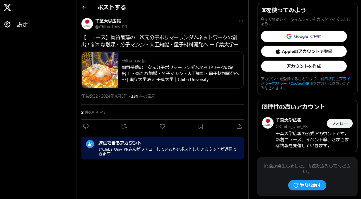
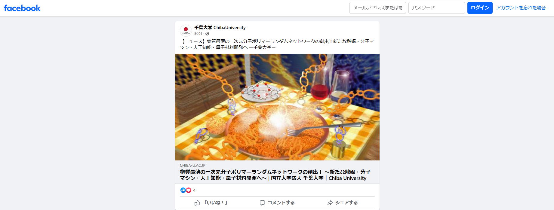
物質最薄の一次元分子ポリマーランダムネットワークの創出! ~新たな触媒・分子マシン・人工知能・量子材料開発へ~
 ニュースリリース PDF.
千葉大HP, Chibadai Next, PRtimes, Twitter(X), Facebook.
【Press Release】論文はこちら!
Small Yet Mighty: Showcasing Precision Nanocluster Formation with Molecular Traps
 【EurekAlert!】【CHIBADAI NEXT】【大学HP】【X】【Facebook】
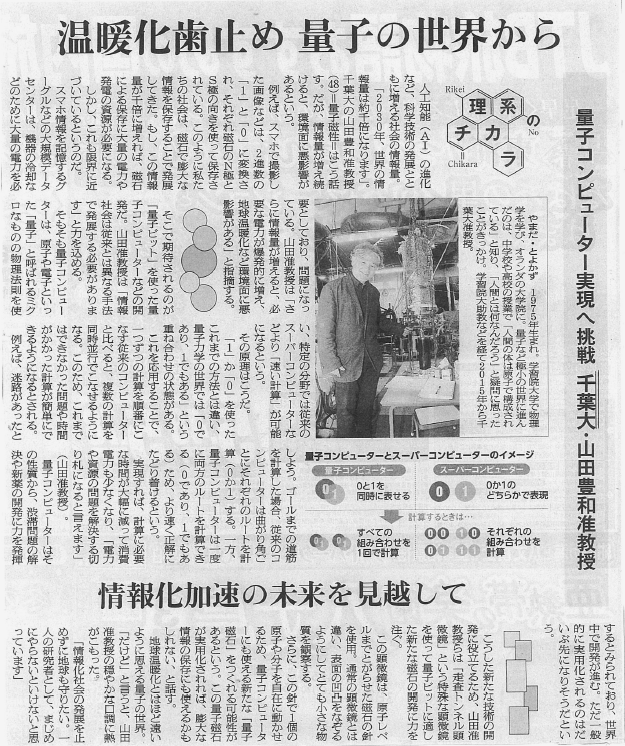
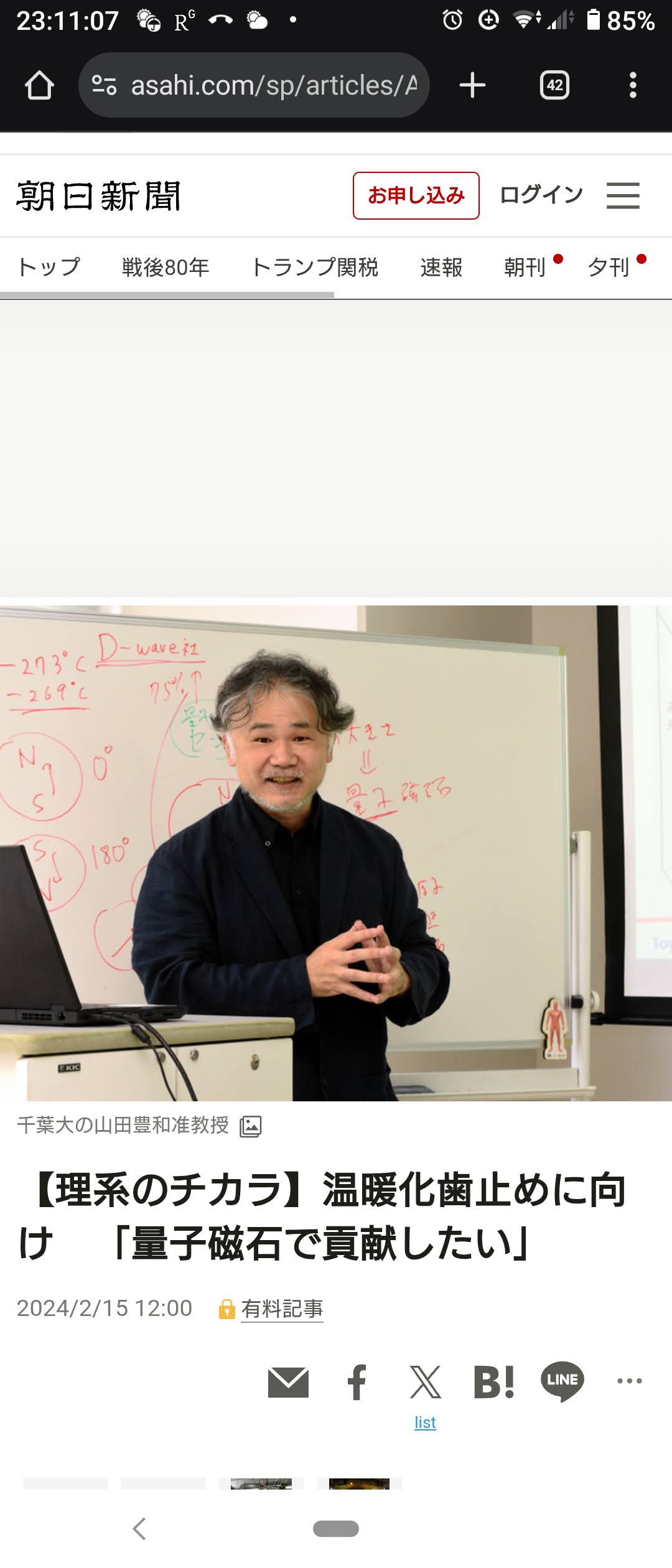
2023年12月16日朝日新聞
【理系のチカラ】温暖化歯止めに向け「量子磁石で貢献したい」」
 【Press Release】論文はこちら!
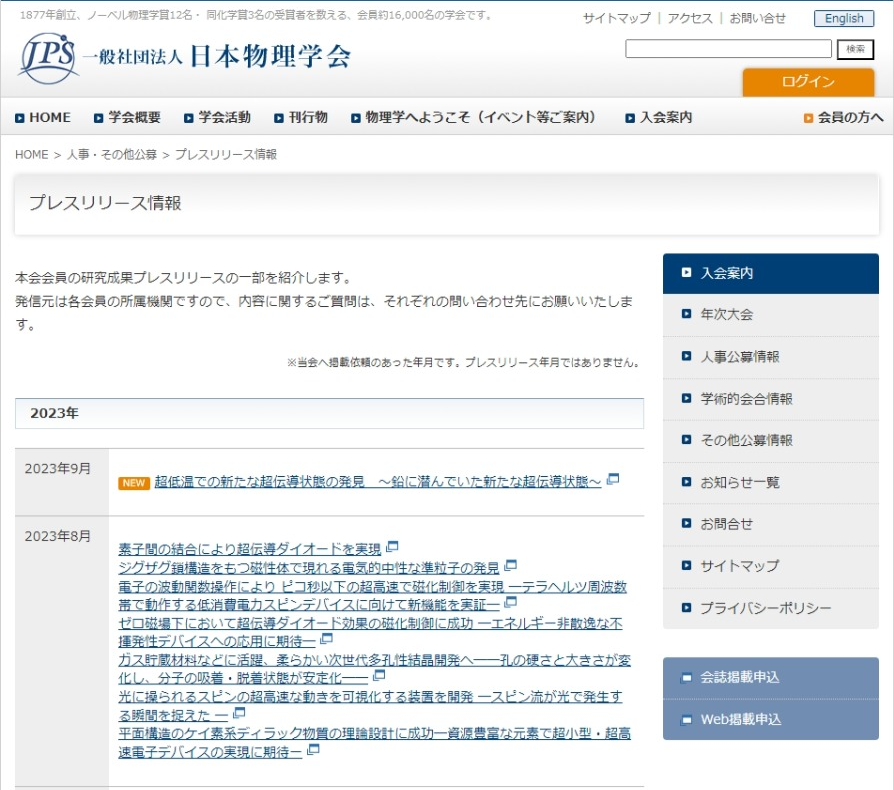
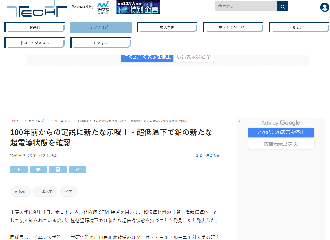
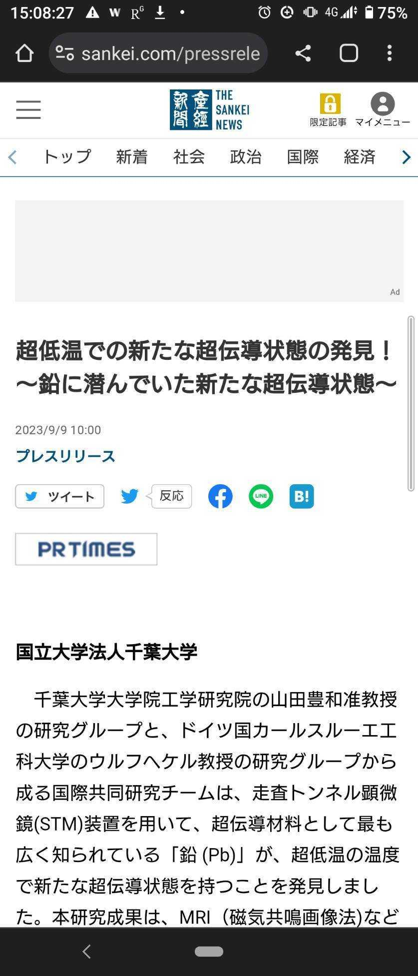
超低温での新たな超伝導状態の発見!~鉛に潜んでいた新たな超伝導状態~
 【Press Release】論文はこちら!
超伝導探針と分子磁石による準粒子の新たな創出手法を開発!~未来の量子コンピューター開発へ~
 【Press Release】論文はこちら!
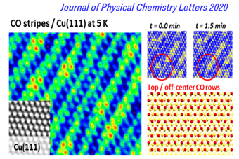
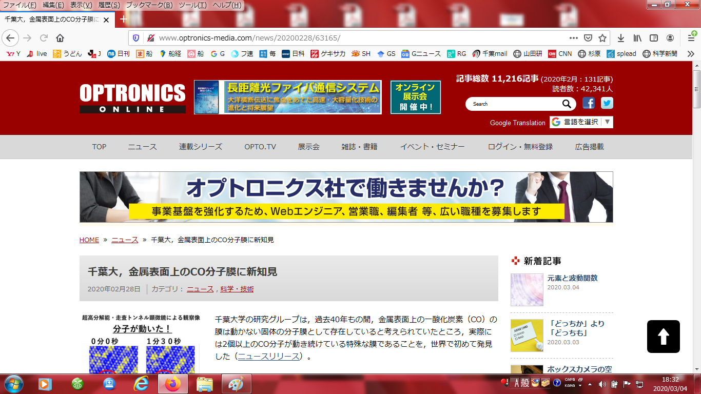
一酸化炭素分子は金属表面上で動いている:銅の単結晶・超高真空・極低温条件による初検出
 【Press Release】論文はこちら!
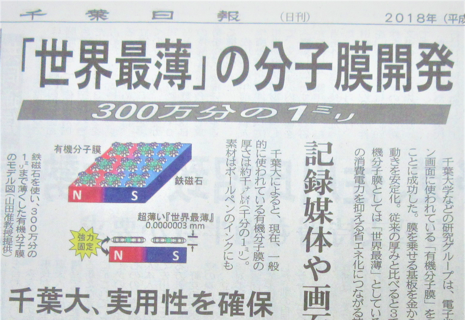
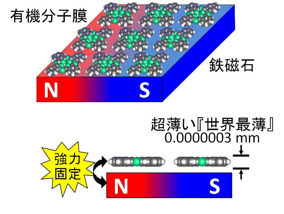
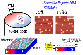
室温でも超安定!「世界最薄」有機分子膜を実現~磁石のパワーで分子膜を強力固定~
【特許取得】
 【Press Release】論文はこちら!
1個の鉄原子で情報記録に成功!~世界最小・ナノ分子磁気メモリ~
 【Press Release】論文はこちら!
インクの分子で、世界最小・磁気センサーの開発に成功!
 【Press Release】論文はこちら!
ナノスケールの鉄磁石を電界でコントロール!
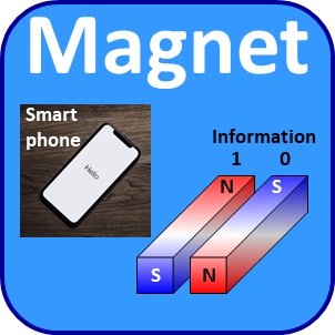
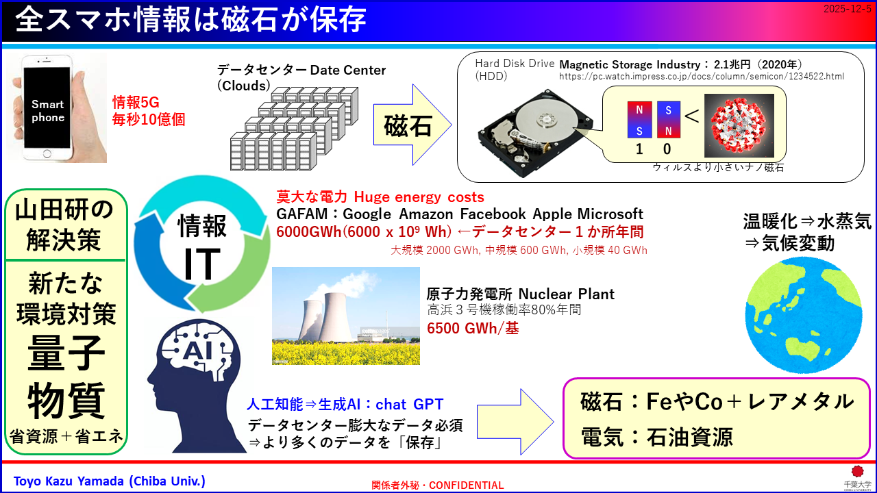
【2】磁石と情報:全スマホ情報を磁石が記憶!
スマートフォンやパソコン(PC)の情報データは、全て「1」と「0」の二進数に変換されます。1個の情報が 1 bit(ビット)です。8 bitが1B (bite: バイト)、1Bで28 = 256個の情報を記述することができます。ひらがな、片仮名、アルファベット、全て1バイトで表記可能です。
全ての情報を、現在、GAFAM (Google, Apple, Facebook, Amazon, Microsoft)等の大規模データセンターの、ハードディスクドライブ(HDD)内の無数のナノ磁石NS極が「記憶」しています。HDDは単価が1GBあたり0.05 ドルと、SSD等の半導体記憶素子 (1.4ドル/GB)と比較し圧倒的に安価です。
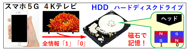
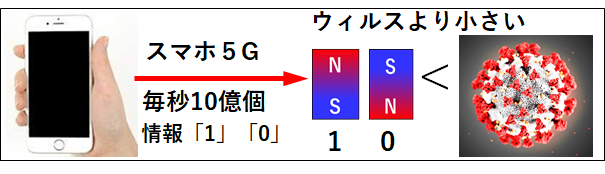
5Gでは、毎秒10億個(=109)以上の情報が伝送できます (1 G bps)。4Kテレビでは、毎秒1億個 (= 108 = 画素 4000 x 2000 x16枚/秒) の情報が伝送されます。そのため、世界で飛び交う日々の情報量は2030年には1024(ヨタ yotta)個」に達すると予想されています。
情報記憶に使用されている、「ハードディスクドライブ(HDD)」は、手のひらサイズ:直径約3.5 inch = 約8.9 cmです。 現在2TB(テラバイト) = 約1012個の情報が保存できます。あらゆるデバイスの大きさは、「ムーアの法則」に従い、この20年で10000倍以上小さくなりました。 1個の磁石(=1ビット)の大きさは、どのくらいでしょうか。直径8.9cmディスク(円板)の面積を1013個で割れば、1個の磁石の面積は約25x25 nm2」です。「nm」は「ナノメートル」です。「ナノ」は「10-9」です。COVID19コロナウィルスの大きさ (約 80 nm)よりも既に小さいです。
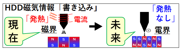 上図にHDD内での磁気情報「書き込み」を示します。無数のナノ磁石が並んでいます。そのわずか「20 nm」上を「磁気ヘッド」が超高速で動き回っています。この感覚は、ジェット飛行機が地面の上、数mmをすれすれで飛び続けていることに匹敵します。現在は、磁気ヘッドから1個1個の磁石に「磁界」を印加します。上図のように鉄などの磁石に銅線コイルを巻き「電流」を流すことで磁界がでます。皆さんがスマホやPCで画面をタッチして「情報を保存」することは「HDD内で磁気ヘッドが高速で動き1個1個の磁石NS極向きを並び替えている」ことを意味します。磁界を出すたびに電流を流すため、コイルが「発熱=電力消耗」します。そのため長時間使用するとPCはどんどん熱くなります。
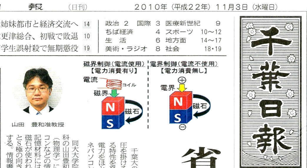
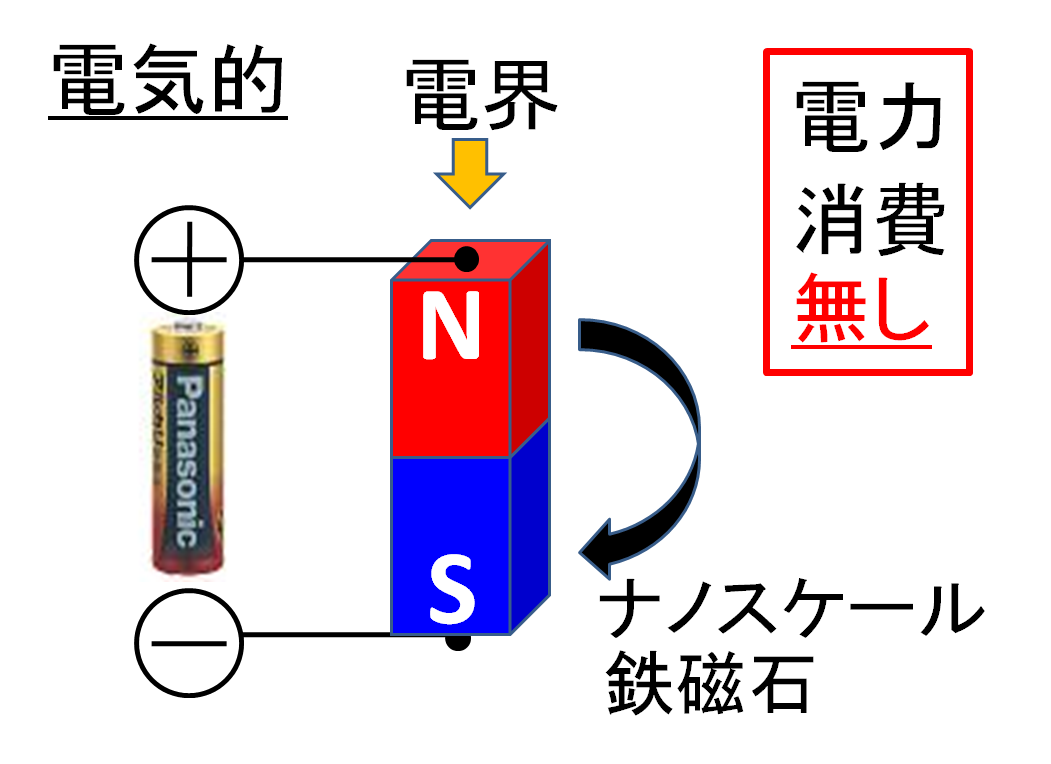
山田ラボでは、2010年代「発熱しない“冷たいPC”」の実現を目指しました。そのためには、磁気ヘッドに「磁界」を使う代わりに「電界」による磁気情報・書き込み手法を実現しなくてなりません。電磁気学では金属磁石に電界は侵入しません。しかし、二原子層厚さまで薄くすれば電界が印加でき、磁石の磁気特性を変化できることがわかってきました。
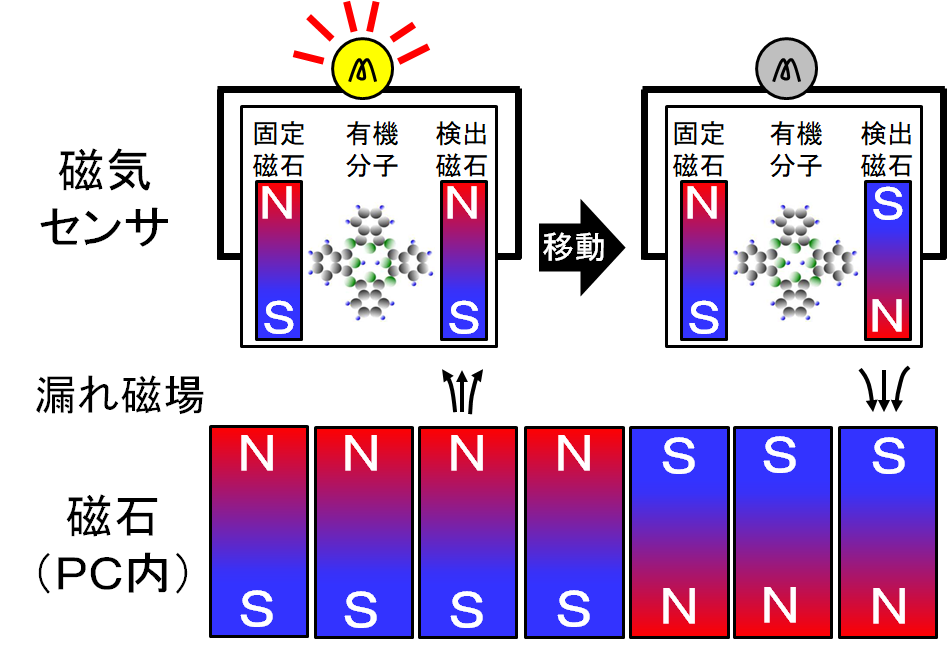
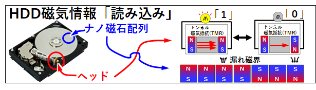
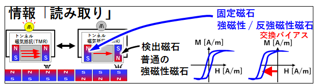
次にHDD内の磁気情報「読み取り」方法を下図に示します。スマホやPCでファイルをクリックします。すると、HDD内では磁気ヘッドが高速で動き、指定個所の磁石NS極並びを読み出し、二進数「1」「0」に変換し、ディスプレイ上に「情報が表示」されます。この「読み取り」を行うのが磁気ヘッドに搭載されている「トンネル磁気抵抗(TMR: tunnel magneto registance)センサー」です。
TMRセンサーは【磁石層 / 絶縁層 / 磁石層】からなり、全体の抵抗値(R)を計測します。「TMRセンサー」は「スピン偏極STM」と同じです【磁石探針 / 真空絶縁層 / 磁石試料】。二つの磁石のNS向きが平行な時、電子スピンのトンネル遷移確率は高くなり (R = 小)、電球が光ります:情報「1」と判別。ところが、磁石の向きが反平行になると電子スピンのトンネル遷移確率は下がり (R = 大) 、電球が消えます:情報「0」と判別。つまり、磁石の向きで電流ONOFFスイッチ制御ができます。これがトンネル磁気抵抗効果です。「磁気抵抗効果」を発見されたPeter Gruenberg博士 Albert Fert博士には、2007年ノーベル物理学賞が授与されました。
HDD内TMRセンサーでは、二つの磁石の内、一方のNS向きは固定されています。これは「反強磁性膜」を「強磁性膜」に付けることで働く「交換バイアス効果」を使って、一方の磁石のNS極向きを固定(ピン)しています。実は「交換バイアス」の原理はいまだによくわかっていません。山田ラボでも15年にわたり原理解明を目指しています。TMRセンサーは、HDDナノ磁石からの「漏れ磁場」 を感じて「方位磁針」のようにクルクル回って情報を読み取っています。
 山田ラボで現在、有機分子を用いた磁気抵抗センサの開発に挑戦しています。
また近年、磁気抵抗センサーは、HDD以外の幅広い分野で活躍しています。TMRセンサーは、いわば「現在の方位磁針」です。GPSセンサーとして、スマホ1台に最低3個 (x, y, z方向) 搭載され、自動運転車1台には20個以上搭載されています。TMRセンサーによる人工知能AI開発など、今後も大きな発展が期待できます。
強磁性膜と反強磁性膜の間の磁気結合の解明:なぜ反強磁性は強磁性を固定する?
磁石は小さくなると「熱揺らぎ」により不安定になります。1個の原子の磁石NS極の向きは「磁気モーメントベクトル [A m2]」です。磁気モーメントベクトルを体積 V [m3]で割ったものが、「磁化ベクトル M (magnetization vector) [V/m]」です。磁石を炎の中に入れて加熱すると、原子の磁気モーメントの向きがばらばらになり、磁化がゼロになります。「消磁」といいます。磁化がゼロになる温度を、強磁性 Fe, Co, Ni では「キュリー温度: TC」、反強磁性 Mn, Crでは「ネール温度: TN」といいます。Fe:1044 K, Co:1388 K, Ni:631 K、Mn:978 K, Cr:312 K。ですから、磁気情報を消すもっとも良い方法は加熱する事です。磁石は原子までばらばらに破壊しても磁気情報は残ります。
温度だけでなく「磁石を小さく=体積を減少」しても、熱揺らぎにより磁化は不安定になります。磁石はどこまでちいさくできるのか?一つの指標となる式があります:Ku V > kB Tです。Ku:ナノ磁石の磁気異方性 [J/m3]、V:ナノ磁石の体積 [m3]、kB:ボルツマン定数、T:温度 [K]。
つまり、小さくしても磁石でいられる「強い磁石」を開発するには、Ku:磁気異方性の高い物質が必要です。現在使われているのは、コバルトCo系:Ku = 4.5 x 10⁵ [J/m3]、鉄白金FePt系:Ku = 7 x 10⁶ [J/m3]です。
原子レベルに薄くても、安定な磁石を作製する新たな方法として、「強磁性膜: ferromagnet (FM)」と「反強磁性膜: antiferromagnet (AFM)」を使う方法があります。まず、普通の鉄などのFM膜のM-Hループ(ヒステリシス曲線)を見てみましょう。上図に示します。外部から磁石の磁化 M [A/m] に磁界 H [A/m]を印加します。すると最初N極を向いていた +M は、逆向きに磁界 -H がかかると、保磁力 Hc を超えると磁化反転します(+M -> -M)。ところが、「不思議なことに」AFM膜に接したFM膜のM-Hループは、下図に示すように変化します。H = 0 において、+Mしか向かなくなります。これが「交換バイアス効果 (exchange bias)」です。磁気メモリー、磁気センサー、GPSに広く使われています。しかし、なぜこんなことが生じるのか、原理は未だによくわかっていません。
【3】走査トンネル顕微鏡 (STM) 原子・分子が見える顕微鏡!
皆さんは、物質最小「原子・分子」を見たことがあるでしょうか?
下図は山田ラボで観察した1個の鉄原子(鉄は磁石です)と、皆さんのボールペンのインクや有機太陽電池にも使われている、四葉のクローバーのように見える、フタロシアニン分子です。これらは、STMを使って観察した像です。【1982年STM誕生。開発者:Binning博士とRohrer博士 1986年ノーベル物理学賞】
STMは探針で試料表面をなぞるようにして表面凸凹をとらえます。ただし、探針と試料は、僅か数原子分(0.5-1.0 nm)しか離れていません。それでも「離れて」います。離れているのに電流が流れます。これが、アインシュタイン博士が発見した量子力学による「トンネル効果」です。そのため、探針と試料にはトンネル電流が流れています。STMは、トンネル電流を検出しながら非接触で試料表面を「原子分解能」で観察しています。
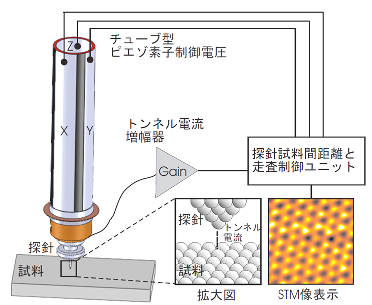 STM測定の回路を右図に示します。探針先端が試料の上、約0.5-1.0nmにあります。この僅か原子数個分の位置を保持しながら探針先端を走査するため、電流ノイズが理論限界4fA/√Hz (fA=10-12A=フェムトアンペア) 程まで低い電流電圧変換増幅アンプ(FEMTO社)とデジタル制御電源Nanonisを使用しています。ピエゾチューブは円筒状の圧電素子です。圧電素子は電圧印加で伸び縮みします。内筒がz方向(高さ)です。外筒は4分割されています。それぞれ+x, -x, +y, -y方向に対応します。+xと-xに逆位相の三角波を印加し、+yと-yにも同様に印加します。x方向に周期は約1Hz、y方向は約(1/500)Hzで、500x500画素の画像取得であれば、だいたい500秒でSTM像が一枚計測できます。
計測したトンネル電流は増幅アンプ(Gain)でだいたい109倍に増幅され電圧信号に変換されNanonisに入ります(右図)。Nanonisでは一般的な定電流モードであれば、指定したトンネル電流値になるようにフィードバックをかけ、ピエゾチューブzへの印加電圧を調整し探針先端位置を制御します。STM形状像は、各画素位置での、ピエゾチューブzへの印加電圧変化をプロットしたものです。
STMの優れた点は、観察だけでなく、その場で「電子分光」を行える点です。各原子の「局所電子状態密度:local density of states」、つまり、デバイス開発で最も重要な「フェルミ準位近傍の電子スピンバンド構造」が直接観察できます。STS:走査トンネル電子分光です。
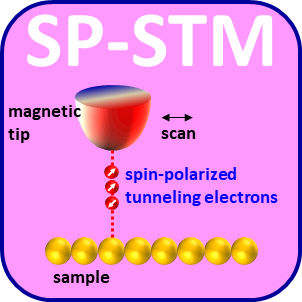
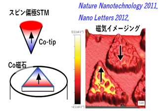
STM/STSの探針として「スピン偏極した磁性探針」を使うと、鉄に代表されるような「磁石」のNS極の向きが可視化できます。これを、「スピン偏極STM (SP-STM)」と呼びます。世界最高の空間分解能 (約 0.5 nm)を有する磁気イメージング手法ですから、原子1個の磁気モーメントベクトル(正確には、スピン偏極度ベクトル)も直接観察できます。山田豊和博士は、SP-STMの第一人者です(2016年SP-STM国際会議主催、2022年IVC真空国際会議委員等)。
 STMを使うと、強い電界をピンポイントで印加したり、超伝導ギャップ計測や量子波の観察など様々な研究が可能です。
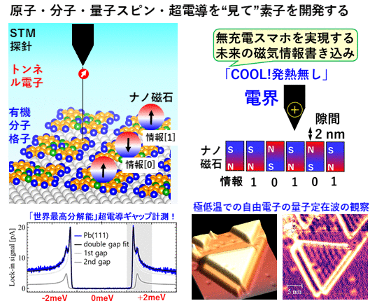
電界印加: 探針と試料の間の距離は原子数個分の約1nm(ナノメートル=10 -9m)です。今、探針と試料間に電圧1Vを印加します。すると、1 V/ 1nm = 109 V/mという巨大な電界を僅か1nmの範囲にピンポイントで印加できます。電界は熱が発生しないため省エネ化が可能です。磁界でなく強い電界を使って磁石の向きを制御する電界スピントロニクスの研究が進んでいます。
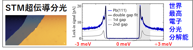
超高分解能電子分光: STS電子分光では、原子レベルの空間分解能で、さらに「μeVエネルギー分解能」で試料の電子状態を計測できます。右図下部は超伝導Pb(111)表面で得た電子分光曲線(超高真空・超低温40mKで計測)です。フェルミオン電子がボゾンのクーパー対を形成したため、フェルミ準位(0eV)の電子状態はゼロになりギャップができています。超伝導になっている決定的な証拠です。
量子波閉じ込め観察: 右図下部には、STM分光像で見た三角形のCu(111)島の中に閉じ込められた、「量子定在波の波」が確認できます。STMを用いると、アインシュタイン博士の発見した量子力学に直接ふれることができます。
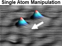
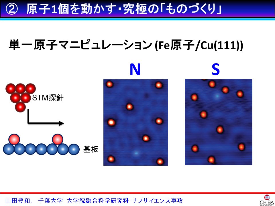
STM原子分子マニピュレーション
STM探針で原子・分子を動かせます。
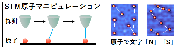
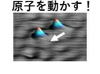 STM探針を使うと1個の原子をつつくようにして動かすことができます。atom manipulation といいます。これが、「究極の物づくり」です。右図はSTM探針をつかって、基板表面にのっかった1個のFe原子をつついて、もう1個のFe原子にくっつけて、人工的に新たな物質(鉄二量体といいます)を開発している動画です。
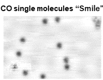
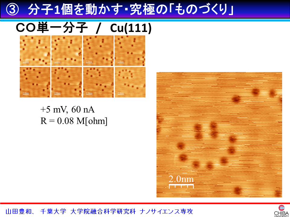
STM分子マニピュレーション
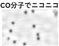 STM探針を使用すると、原子だけでなく「分子」も動かす事ができます。molecule manipualtion と呼びます。右図で、黒く見えている点が、1個のCO分子 (carbon monoxide)です。Cu(111)基板に対しCO分子は炭素C原子がCu原子と結合し、酸素O原子が上向きに直立しています。STM探針からみると、酸素O原子がしか見えません。CO分子位置でのトンネル伝導値は、金属Cu(111)基板より低いため、”見せかけ上”CO分子の高さは低く暗く見えています。STM金属タングステン探針を接近させると、タングステン原子と酸素O原子との間に引力が働きます。タングステン原子に引っ張られるようにして酸素O原子が引っ張られ、CO分子が探針を追うようにして動きます。右図はCO分子10個をつかって”ニコニコ”マークを描いた様子です。
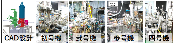
【4】STM装置5台 稼働中!
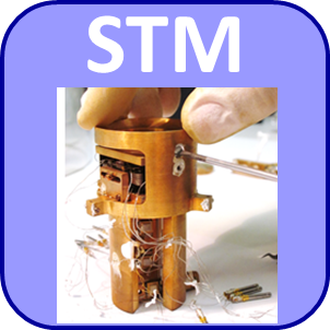
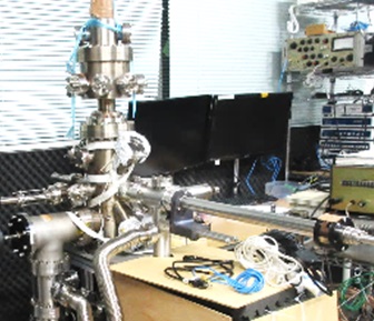
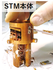 山田ラボではSTM装置を独自にCAD設計して自主開発しています。現在、4台の自作STM装置と1台の市販STM装置が稼働中です。STM本体は右図のように手の平サイズです。しかし、大気中の試料表面には、空気中の分子・原子が吸着しているため、正確に見たい原子分子が観察できません。そのため、STMは1メートルを超える大きな真空チェンバー内にあります。宇宙空間と同じ超高真空・極低温環境を山田ラボで作り出してSTM研究しています。さらに、室温では原子分子は基板表面上で熱拡散してしまいます。二次元膜であれば室温 (300 K = 27 oC)でも観察できますが、1個の分子・原子を観察するには"冷却"しなくてはなりません。
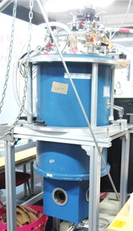
 そこで、クライオスタット冷却器を設置し、液体窒素(77.5 K)と液体ヘリウム4He (4.2 K)を使用して、極低温でのSTM研究を実現しています。ドイツ・スペイン国際共同研究プロジェクトでは、さらに、3He液体ヘリウムを使って「超低温 25 mK」「究極の電子エネルビー分解能:0.025 meV」でSTM観察できます。
千葉大に着任後、様々な装置を開発してきました!
①走査トンネル顕微鏡 (STM):物質表面の原子・分子の実空間観察。
②走査トンネル分光 (STS):原子スケールでの局所電子状態密度計測。
③スピン偏極STM/STS:原子スケールでの磁気情報(スピン偏極度)計測。
④光照射STM:単分子レベルでの光照射反応観察。
⑤原子間力顕微鏡 (AFM):ナノスケールでの物質表面観察。
⑥走査電子顕微鏡 (SEM):ナノからミリスケールでの物質表面観察。
⑦電界放射顕微鏡 (FEM):探針形状物質先端のナノ構造観察。
⑧光学磁気Kerr顕微鏡:マイクロスケールで磁区観察。
 SEMとプローブ伝導計測付き製膜装置 |
FEM装置 |
Spemag |
大気AFM/STM (JEOL4200) |
 Tiny-SEM |
探針化学エッチング装置 |
磁気偏光顕微鏡 |
昇華精製電気炉 |
 VSM磁気計測装置 |
探針炎エッチング装置 |
【5】STM電子分光:電子状態密度計測
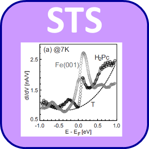
STM探針を使って、原子レベルの空間分解能で試料フェルミ準位近傍の局所電子状態密度計測が可能です。これを、走査トンネル分光法 (STS: scanning tunneling spectroscopy) と呼びます。
下図にイメージ図を示します。学生の皆さんも学生実験でテスターを使って、プローブ先端を押し当てて電気抵抗を計測したことがあると思います。同じような感覚で、ただし原子レベルでとがった探針をプローブとして、試料の上わずか1nmで試料にぶつけずに探針を固定して、試料に印加する電圧(V)を変化して探針と試料間の流れるトンネル電流(I)の変化を計測します。I-V曲線が得られます。これを数値微分すると、トンネル微分伝導: dI/dV曲線が得られます。ロックインアンプを使用すると直接微分伝導が得られます。
下図の左から二つ目の図は、実際に1個の分子の上で計測したdI/dV曲線です。0Vがフェルミ準位。正電圧側が試料の非占有状態密度(伝導帯やLUMO)です。負電圧側が試料の占有状態密度(価電子帯やHOMO)です。 STSの利点は、dI/dV曲線と同時に、各電圧での分光マッピングが可能です。下図の右二つはHOMOとLUMOの空間分布を示しています。HOMOやLUMOが分子配列の各分子位置に局在していることが分かります。
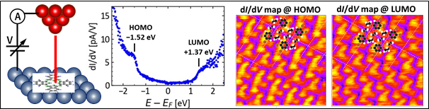
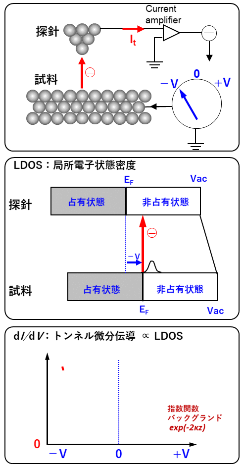 右の動画でSTS測定の概要を説明します。上から、回路図、探針と仕様の電子状態密度の間のトンネル電子の遷移の様子、実際に計測されるdI/dV曲線、です。
フィードバックを切り探針先端位置を固定します。試料の電圧を変化します。負電圧では試料から探針へ。正電圧では探針から試料へトンネル電子が流れます。いま、試料の非占有状態に電子状態ピークがあるとします。するとここでだけ電子が多く流れます。その結果、dI/dV曲線の正電圧の位置にピークが現れます。
右の動画でSTS測定の概要を説明します。上から、回路図、探針と仕様の電子状態密度の間のトンネル電子の遷移の様子、実際に計測されるdI/dV曲線、です。
フィードバックを切り探針先端位置を固定します。試料の電圧を変化します。負電圧では試料から探針へ。正電圧では探針から試料へトンネル電子が流れます。いま、試料の非占有状態に電子状態ピークがあるとします。するとここでだけ電子が多く流れます。その結果、dI/dV曲線の正電圧の位置にピークが現れます。
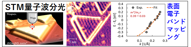
量子波: 表面バンド分散
極低温の世界では熱揺らぎは抑制されます。すると、電子の波の特性、「量子波」をSTM分光像で観察できます(下図)。 下図はCu(111)表面上の三角形の島で、STM電子分光マッピングを行った結果です。 右からSTM形状像(3D)、電子分光像、E-k曲線です。電子分光dI/dV像では、三角形の島の中に閉じ込められた電子が量子の波を形成していることが分かります。電圧を変化しながら波の周期λ [m]を求めます。逆数をとると逆格子空間(k空間)の面内成分 k||が得られます。下図の右図は、縦軸にエネルギー、横軸にkをとったものです。自由電子(4s電子)は二次関数バンドを形成していることが分かります。
【6】スピン偏極STM: 原子レベルでの磁気イメージング
1990年代、STMで原子が見えたのだから、次は「原子のスピン磁気モーメントベクトル(正確には、スピン偏極度ベクトル)を見たい!」、という機運が高まり、欧米や日本で大型国家プロジェクトが立ち上がりました。当時の主流は、半導体GaAsに円偏光を照射し励起されるスピン偏極電子流を利用する手法でした。結果、全ての研究プロジェクトは失敗しました。
ところが、2000年「革命」が起きました!ドイツ・ハンブルグ大学のRoland Wiesendanger博士と Mattias Bode博士が、磁性金属薄膜を使った「スピン偏極STM探針」を使って、原子の磁気配列をとらえることに成功しました。 画期的ポイントは、広く使用されていた非磁性で高融点物質のタングステンSTM探針を超高真空中でフラッシングすることで (探針先端のみ数秒2300 K加熱)、曲率半径約100-200 nmの平坦で清浄な先端表面にしてから磁性薄膜を蒸着し、探針先端に自発的「スピン偏極度ベクトル」を持たせることに成功した点です。山田博士は、2003年Mn/Fe(001)系で、室温スピン偏極STM計測に成功しました。下図にこれまで山田博士を含めたSP-STM研究者が開発してきたスピン偏極探針の一覧を示します。また、2021-2022年には超伝導を使った新たなスピン偏極探針が開発されています。Nb探針先端に磁性原子や分子を吸着するとYu-Shiba-Rusinov(YSR)状態が発現します。このYSR状態は原理的には100%スピン偏極しています。
SP-STM形状測定モード
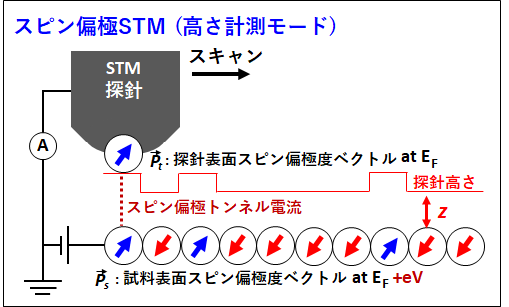 右図がスピン偏極STMの高さ変化計測のモデル図です。探針と試料の原子の磁気モーメントベクトル(=スピン偏極度ベクトル)は、平行であればトンネル遷移確率が増し電流がおおく流れ、反平行であればトンネル遷移確率は減り電流量は下がります。ですから、定電流モードであれば、平行の位置は高く、反平行な位置は低く観察されます。この高低差が磁気コントラストであり、STM形状像の中に磁気情報が入って観察できます。
SP-STM分光モード
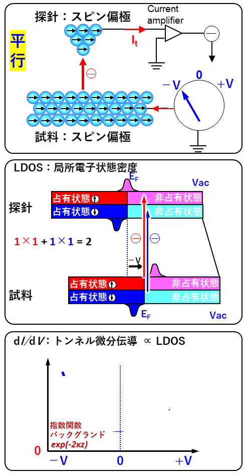 上記のSP-STM形状測定モードでは、形状像の中に磁気情報が混在しています。1個の原子分子など高い空間分解能が必要なSP-STM計測では有効ですが、できれば形状像と磁気像を分離して計測したいです。そこで考え出されたのが、右の動画に示すSP-STM分光モードです。
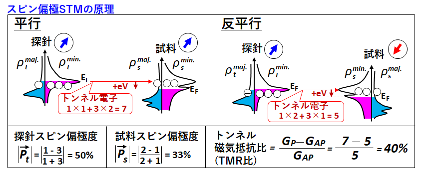
原理は通常のSTM分光と同じです。違うのは探針も試料も磁石であるため、電子状態密度がスピン偏極している点です。アップスピンとダウンスピンの電子状態密度、それぞれのトンネル遷移を考える必要があります。でも、難しくはありません。トンネル遷移過程において、スピンフリップはないです。アップスピンはアップスピンの電子状態密度へ、ダウンスピンはダウンスピンの電子状態密度にしか移れません。
右動画では、アップとダウンスピン電子状態密度、それぞれにピークがあります。正電圧では、試料フェルミ準位のアップスピン電子状態密度ピークから探針非占有スピンアップ電子状態密度ピークへ、より多くの電子が遷移します。 すると、この電圧位置でdI/dV曲線は高い強度のピークを示します。
探針と試料のスピン偏極度ベクトルが、平行・反平行で、アップスピンとダウンスピンの遷移確率が変化するため、ピーク強度も平行では大きく、反平行では小さくなります。この強度さが磁気コントラスト(dI/dV平行 - dI/dV反平行 )です。さらに、この差をこの和で割ったものが非対称(asymmetry)です。AdI/dV = ( dI/dV平行 - dI/dV反平行) / ( dI/dV平行 + dI/dV反平行)です。さらに、AdI/dVは、試料と探針のスピン偏極度ベクトルの内積に比例します。定量的に試料スピン偏極度を得るには、探針スピン偏極度を知ることが必要です。 下図に詳しいスピン遷移を示した。
 磁気イメージング
SP-STM分光モードを使って、形状像と磁気像を分離して計測した結果を下図に示します。
磁気像では磁気コントラストが試料の磁気情報を示します。明るい場所が探針スピン偏極度ベクトルと平行、暗い部分が反平行です。磁気コントラストは、試料と探針のスピン偏極度ベクトルの内積に比例します。つまり、cosθで変化します。θは試料と探針のスピン偏極度ベクトルの角度です。
磁気イメージング
SP-STM分光モードを使って、形状像と磁気像を分離して計測した結果を下図に示します。
磁気像では磁気コントラストが試料の磁気情報を示します。明るい場所が探針スピン偏極度ベクトルと平行、暗い部分が反平行です。磁気コントラストは、試料と探針のスピン偏極度ベクトルの内積に比例します。つまり、cosθで変化します。θは試料と探針のスピン偏極度ベクトルの角度です。
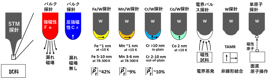
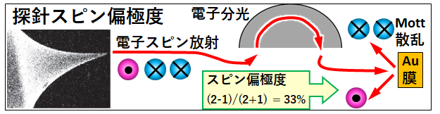
磁性探針スピン偏極度計測 SP-STM計測から磁気コントラストが得られたとします。これから、試料スピン偏極度を定量的に求める手法を説明します。dI/dVの非対称(asymmetry)を求めます。AdI/dV = ( dI/dV平行 - dI/dV反平行) / ( dI/dV平行 + dI/dV反平行)です。これが試料と探針のスピン偏極度ベクトルの内積に比例します。ですから、定量的に試料スピン偏極度を得るには、探針スピン偏極度が必要です。山田博士は、下図に示すMott検出器を用いて探針先端のスピン偏極度計測を実施してきました。Fe/W tipは44%、Mn/ W tipは10%でした。
【7】光照射STM:分子の光化学反応
光STM (light-illumination STM, LI-STM)の始まりは、2000年代、STMを使って有機分子からの「発光」を、カリフォルニア大学バークレー校Wllson Ho博士が原子分解能でとらえたことに始まります。光検出STMの誕生です。原理は、有機ディスプレイとして広く市販されている有機EL (electro luminessence)と同じです。その後、2010年代、筑波大・重川先生グループが、STM試料への光照射研究を重点的に実施され「光照射STM」の礎ができました。
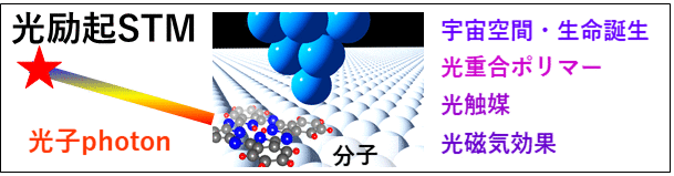 山田ラボでも「光照射STM」を独自開発しています。超高真空・極低温STM装置の試料近傍に「光ファイバー」を設置します。これにより超高真空・極低温環境を保持したまま光を試料に照射できます。
分子マシン 光などの外部刺激により、分子構造が変化する有機分子があります (例、シス-トランス)。「分子ナノロボット、分子マシン」とも呼ばれます。 分子マシンは、生命・化学・物理の幅広い領域の発展に多大な影響を与えるとして、2016年ノーベル化学賞が発見者:Jean-Pierre Sauvage博士, J. Fraser Stoddart博士, Ben L. Feringa博士に授与されました。
分子マシンは、外部刺激(光・熱・電界等の外的エネルギー)により駆動し、分子構造が変化します。この機械的運動を使うことでロボットのように分子を駆動できます。これまで主に、分子ロボットは血管内での薬デリバリーを目指し、溶液中でマイクロスケール(10-6 m)の生命分子を中心に研究が進んできました。一方、溶液中では1個の分子の自由度が高すぎ、熱拡散で規則的制御は極めて困難でした。デバイス化するには、基板表面に吸着する必要があります。そこで、基板表面上で、直接、分子マシンを組み立てていく手法に挑戦しています。分子マシンに磁性原子を含めておけば「動く磁石」が実現できます。
「光触媒」「光重合ポリマー」 など、単分子レベルで「光化学反応」を直接STM観察することで、新たな光制御型・ナノ分子デバイスを開発します。上記の表面場合成は「熱エネルギー」を使用しました。同様に分子は紫外線などの光にも反応します。とくに、Pt、Pd、Rh等の貴金属表面場を用いれば、有機分子は光触媒反応により、より低い活性化エネルギーで別の分子に変化します。光触媒効果も利用し、新たな磁性MOFの開発を目指しています。
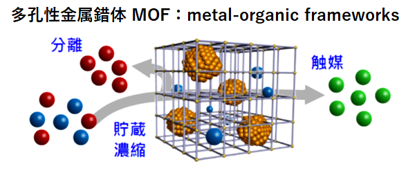 光触媒:磁性MOFと紫外線照射による二酸化炭素分子の分解
さらに、磁性原子と有機分子の構造体は多孔質物質です。触媒金属表面で原子分子構造体を創ることで、効率的にCO2分子を取り込み活性な磁性原子は光触媒反応でCO2を分解します(単原子触媒: single atom catalysts)。新たな温暖化防止物質を開発しています。
【8】表面場での新たな分子磁石合成
Atom-by-atom
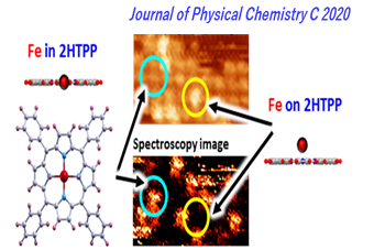
山田ラボでは「表面場」という新たな反応場を用いて、溶液中合成では数年かかるような合成(または実現不可能な合成)を、僅か数日の短期間で合成し、新たな物質創出に挑戦しています。例えば、インク分子や有機太陽光発電にも使用されるフタロシアニン分子(Pc, 四葉の形)を挙げます。溶液中合成では「2HPc + Fe -> FePc + H2 (gas)」の反応が生じます。しかし、表面場では、水素脱離を伴わない「2HPc + Fe -> Fe-2HPc」の合成も可能です。さらに、酸素・窒素等の元素原子で終端した分子を介して磁性原子を連結する方法に挑戦中です。1個1個の原子分子を動かし、新たな超分子を作り上げる手法が、atom-by-atomです。
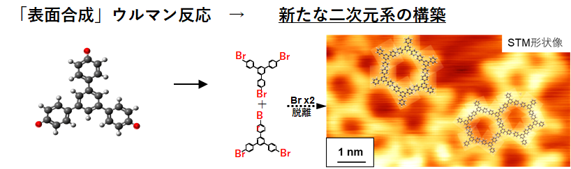
ウルマン反応
また、ハロゲン元素(ヨウ素I、臭素Br、塩素Clなど)が終端した分子を前駆体として使うとどうなるでしょうか?表面場にこれらの前駆体分子を吸着した後、真空加熱します。すると、前駆体分子は表面基板上を熱拡散しながら、ハロゲン元素が脱離します。手が切れた炭素原子を持つ分子が、別の前駆体の同じく手が切れた炭素原子と出会えば、新たな共有結合を形成します。これが繰り返され大きな分子構造体ができます。もっとも成功している例が、表面場を用いた多様なグラフェンナノリボンの合成の成功です[Cai et al., Nature 466, 470 (2010); Wang et al., Nature Reviews Physics, 3, 791 (2021)]
山田ラボでは、ハロゲン原子終端したトリスベンゼン分子やクラウンエーテル分子など、多くの前駆体分子と磁性原子を組み合わせ、新たな二次元磁性金属有機構造体(磁性MOF)の研究開発を実施しています。
人工知能材料 金ナノ粒子とカーボンナノチューブと磁性原子によるニューラルネットワーク作製と発火現象
人の脳は僅か20 W(ワット)の消費電力です。皆さんも自分の頭を触ると発熱量がわかります。ほんのり温かい程度です。一方、スマホやパソコンを使っていると脳よりずっと熱くなります。つまり、電力消耗が大きいのです。ですから、もし、人の脳に近いデバイスができれば、ものすごい省電力化が実現します。実際、IBM社が開発した人工知能Watsonを駆動するの必要な消費電力は1,000,000 Wです。
人工知能を実現するには、人の脳の信号伝達である神経バイパスをまねた「ニューラルネットワーク」が必要です。我々は、これまで研究してきた、金微粒子、磁性原子(鉄酸化物)、ナノカーボン材料を使って「ニューラルネットワーク」を作製し、人と同じような「発火現象」を伴う伝導特性の実現に挑戦します。
生物の情報伝達も電気伝導です。通常は極めて低い電気信号ですが、手をぶつけたり、激辛なものを食べた際、伝導が急に跳ね上がります。「発火」と呼びます。発火して閾値を超えると、脳内の神経経路を伝って信号が伝達していき、我々は「痛い」「辛い」と感じます。 「発火」は、「確率共鳴」により生じます。通常の電気の流れ(伝導)に、「ノイズ」が混在することで生じます。このような、「伝導」+「ノイズ」で、人工的に確率共鳴を起こし「発火」を実現することに、共同研究者の田中啓文先生のグループが成功しました [Tanaka et al., Nature Communications (2017)]。山田ラボでは、これまで培ってきた「カーボンナノチューブ (CNT)」「グラフェンナノリボン (GNR)」「磁性原子」を駆使して、神経模倣デバイスの開発に挑戦しています。
「宇宙」空間での物質誕生を知りたい!~
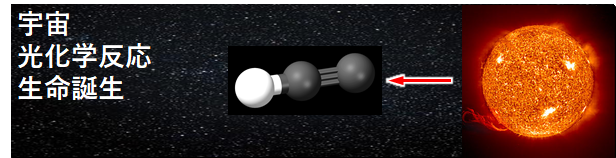
宇宙空間には、現在までに 200種を超える有機物があります。炭素鎖分子が存在しています。ニチニルラジカル (CCH)や、シアノジアセチレン (HC5H)があります。また、宇宙空間は超高真空です。温度は基本 10 K以下の極低温環境です(摂氏ゼロ度 0 ℃ = 273.15 K)。太陽などの恒星の周囲でも数十ケルビンしかありません。山田ラボでは「宇宙空間と同じ」環境の超高真空・極低温装置があります。さらにSTM観察しながら光照射することで、宇宙での有機物の化学反応や物質誕生の解明にも挑戦しています。極低温・超高真空環境・表面場での、生命に必要な4元素である水・アンモニア・メタン分子へのUV照射によるタンパク質分子合成にも挑戦しています。
【9】 量子コンピューターを実現する量子ビット開発:超伝導と磁石
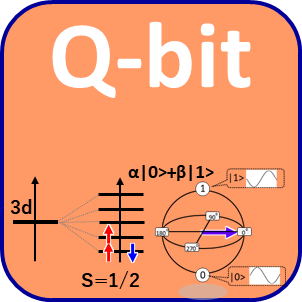
量子ビット 温暖化の解決策の一つに、2012年ノーベル物理学賞「量子科学技術の発展」があります。
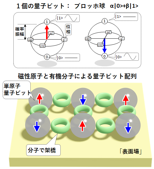 いわゆる「量子コンピューター」です。量子コンピューターには、情報を制御する「量子ビット」が必要です。じつはこの量子ビットも「1個の磁石の原子」で実現できます。磁石は物質最小1個の原子になっても磁石です。1個の磁性原子になることで、電子軌道の縮退が解け量子状態に分裂するので、1個の原子が1個の量子ビットになります。量子ビットのユニークな点は、単純な|1>と|0>ではなく、その二つが合わさった α|1>+β|0> の形で表記できる点にあります。さらにαはα=A(cosθ+i sinθ)の「波」です。ですから、現在の1ビット磁石ではN-SとS-Nの2個の情報しか制御できませんが、量子ビットは確率振幅Aや位相θを変えることで多様な情報を表現できるので、未来の情報素子として期待され世界中で研究が進んでいるのです。
例えば、3個の量子ビットを用いれば、α|000> + β|001> + c|010> + d|100> + e|110> + f|101> + g|011> + h|111>の波の重なりとして表記できます。現在までに既存の超伝導回路を使った量子アニーリング計算は始まっていますが(D-wave社約5000量子ビット)、既存の古典ビットのギガ(109)からテラ(1012)量子ビット実現には程遠い状況です。
磁性原子の”準安定”二次元配列を有機分子格子で実現
基板表面に吸着した単原子・単分子を、外部刺激エネルギー(STM探針からの電界・加熱・光照射)を使い自在に操り結合させ、新たな二次元磁性原子分子配列を創り出します。特に、あえて「磁気フラストレーション」を含んだ準安定な二次元磁性原子格子は、量子アニーリング計算で考えられている原子磁石イジングモデルそのものです。
例えば、交通渋滞や最適な人員の配置など、1つずつ組み合わせを試さなくては解決できない「組合せ最適化問題(いわゆるNP問題)」は、既存の古典コンピューターでは無限に近い膨大な時間(t)を要します。しかし量子アニーリング計算では解が短時間(√t)で得られます。これを実現するには準安定な「磁気フラストレーションを含む二次元量子ビット配列」が必要です。量子アニーリング計算では、まず全原子のスピンを同方向に揃え、それから各原子間の磁気結合によって最終的な向きが決まり(アニーリング)、解を得ます。もし、全ての磁気結合(J)が同じなら毎回解は同じとなり計算になりません。「あえて」磁気フラストレーションを与え、各原子間の磁気結合が毎回変化し、スピン方向が毎回どちらを向くか分からない「準安定な二次元系」が必要なのです。そのような系が実現可能でしょうか?
有機分子を上手く活用することで超高密度化への道が切り拓かれます。山田ラボでは、ボトムアップ式で、表面場で有機分子と磁性原子が結合し、準安定な磁気フラストレーションを含んだ二次元系の構築に挑戦しています。
本研究では、磁性原子は動きやすいので有機分子を用いて固定し、また分子長で原子間距離を調整します。磁性原子の磁気異方性や電子スピン状態は基板の局所結晶場で決まります。では、分子と結合するとどうなるでしょう。基板の結晶場に、さらに分子の配位子場が加味されます。磁性原子の3d軌道や4f軌道の縮退はとけ離散します。そして離散した各量子軌道にアップスピン・ダウンスピンが入り、原子全体のスピン角運動量ベクトルが決まります。量子ビットとしては、|1>と|0>の二準位系が欲しいです。また、離散した軌道間のエネルギー差は 0.01 meV - 1 meVと非常に小さい場合が多いです。このため、離散した軌道を計測するためには、STM電子分光を極低温(4Kでは約0.35meVのエネルギー分解能)から超低温(0.04Kでは約0.0035meVのエネルギー分解能)で行う必要があります。
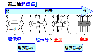
超伝導 多くの物質は4K以下に冷却すると超伝導になります。そのため、超伝導と磁性原子の磁性理解も重要です。下図は超伝導表面でのSTS計測です。超伝導は、電子と電子が結合して電子対を作ります(クーパーペア)。その際、結合・反結合軌道ができるため、フェルミ準位近傍に僅か1meVほどのギャップが開きます。超伝導ギャップです。極低温STSでは超伝導ギャップが観察できます。この超伝導ギャップ内にできる準位が「準粒子」や「Yu-Shiba-Rusinov(YSR)状態」です。超伝導というマクロな状態に保護されているため不純物原子等の影響はうけにくく高い耐久性があります。トポロジカル量子コンピューターを実現するための重要な鍵と考えらえています。
トポロジカル超伝導による準粒子
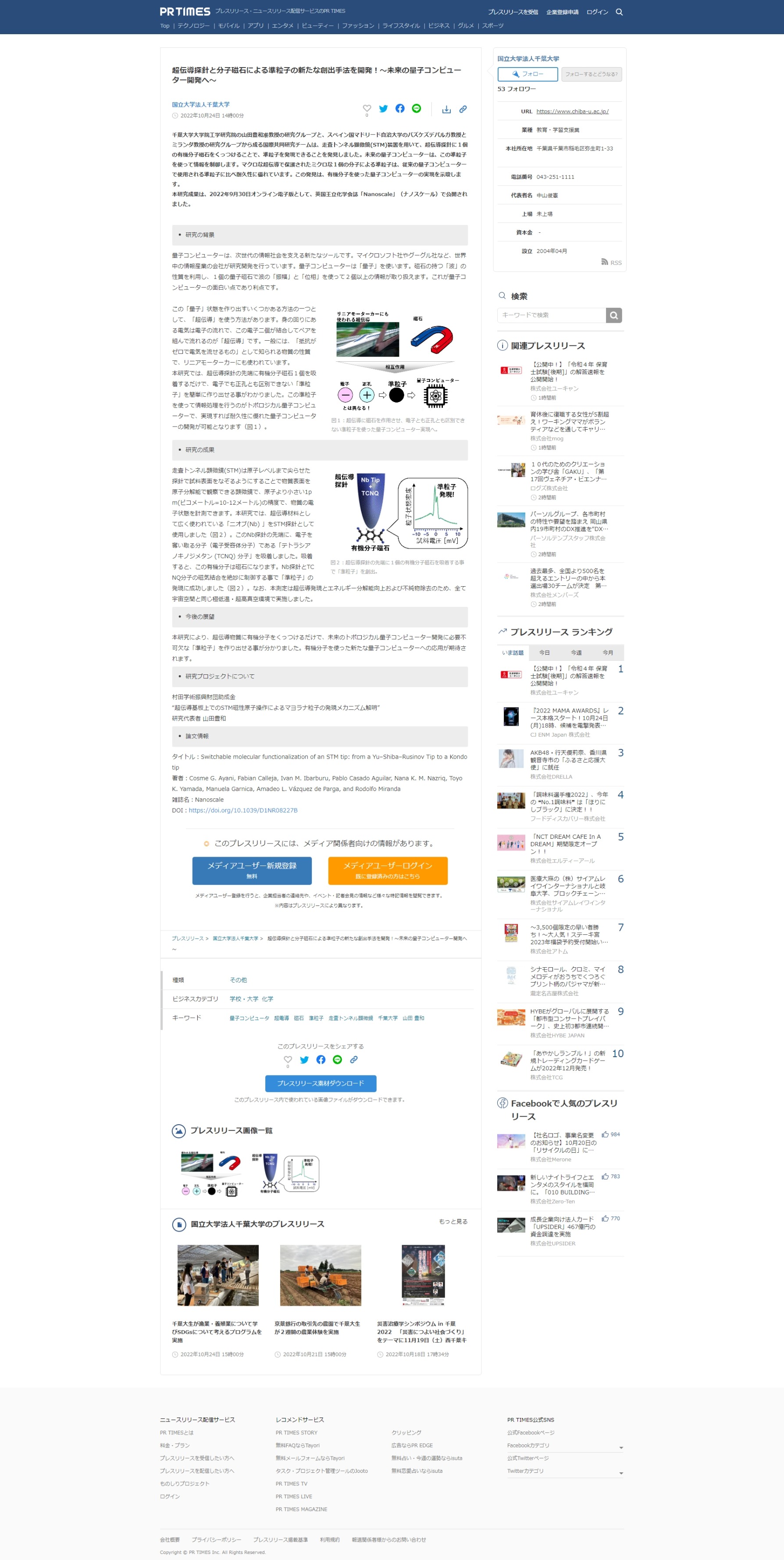
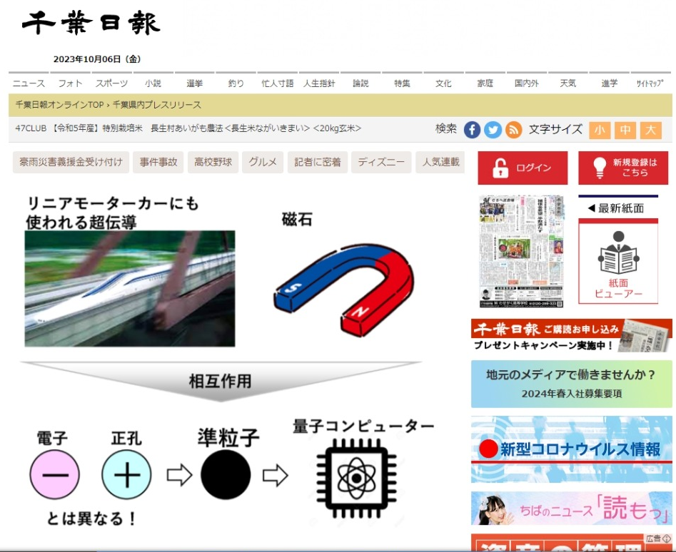
量子コンピューターは、次世代の情報社会を支える新たなツールです。マイクロソフト社やグーグル社など、世界中の情報産業の会社が研究開発を行っています。量子コンピューターは「量子」を使います。磁石の持つ「波」の性質を利用し、1個の量子磁石で波の「振幅」と「位相」を使って2個以上の情報が取り扱えます。これが量子コンピューターの面白い点であり利点です。
この「量子」状態を作り出すいくつかある方法の一つとして、「超伝導」を使う方法があります。身の回りにある電気は電子の流れで、この電子二個が結合してペアを組んで流れるのが「超伝導」です。一般には、「抵抗がゼロで電気を流せるもの」として知られる物質の性質で、リニアモーターカーにも使われています。
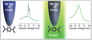
本研究では、超伝導探針の先端に有機分子磁石1個を吸着するだけで、電子でも正孔とも区別できない「準粒子」を簡単に作り出せる事がわかりました。この準粒子を使って情報処理を行うのがトポロジカル量子コンピューターで、実現すれば耐久性に優れた量子コンピューターの開発が可能となります(下図)。
研究の成果 走査トンネル顕微鏡(STM)は原子レベルまで尖らせた探針で試料表面をなぞるようにすることで物質表面を原子分解能で観察できる顕微鏡で、原子より小さい1pm(ピコメートル=10-12メートル)の精度で、物質の電子状態を計測できます。本研究では、超伝導材料として広く使われている「ニオブ(Nb)」をSTM探針として使用しました。このNb探針の先端に、電子を奪い取る分子(電子受容体分子)である「テトラシアノキノジメタン (TCNQ) 分子」を吸着しました。吸着すると、この有機分子は磁石になります。Nb探針とTCNQ分子の磁気結合を絶妙に制御する事で「準粒子」の発現に成功しました。なお、本測定は超伝導発現しとエネルギー分解能向上および不純物除去のため、全て宇宙空間と同じ極低温・超高真空環境で実施しました。
本研究により、超伝導物質に有機分子をくっつけるだけで、未来のトポロジカル量子コンピューター開発に必要不可欠な「準粒子」を作り出せる事が分かりました。有機分子を使った新たな量子コンピューターへの応用が期待されます。
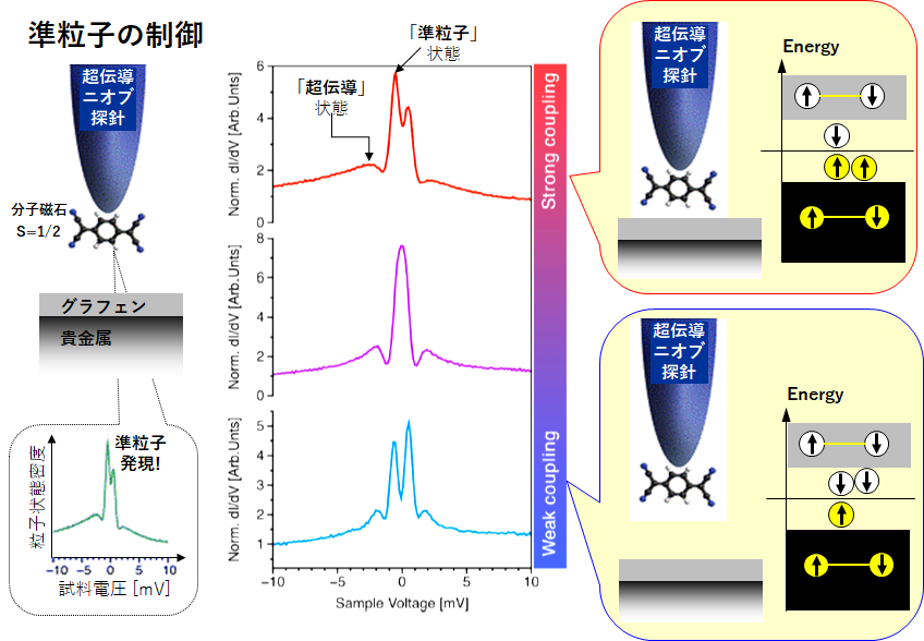 論文タイトル:Switchable molecular functionalization of an STM tip: from a Yu-Shiba-Rusinov Tip to a Kondo tip
著者:Cosme G. Ayani, Fabian Calleja, Ivan M. Ibarburu, Pablo Casado Aguilar, Nana K. M. Nazriq, Toyo K. Yamada, Manuela Garnica, Amadeo L. V?zquez de Parga, and Rodolfo Miranda
雑誌名:Nanoscale
DOI:https://doi.org/10.1039/D1NR08227B
【10】Publications : 研究論文・解説・書籍・特許等
山田ラボでは、研究成果を「論文・解説・書籍・特許」にして世界に発信しています。ぜひクリックしたり、PDFファイルをご覧いただき「世界最先端の研究の世界」を体感してください!
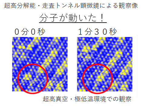
 Cu(111)表面上のCO分子膜は動き続けていることが判明!40年間、固まってると思われていました。 |
 世界で初めて、ポルフィリン分子と磁性原子がくっつき化学反応が起こる前の状態の直接観察に成功! |
 特殊な式をつかうことで水晶振動子(QCM)で分子を厚さ[m]でなく、1個ずつの個数で吸着制御できます! |
 非常に柔らかい環状クラウンエーテル分子の二次元規則(7x4)配列をCu(111)表面で実現! |
 鉄をつかうと、分子を止められます!室温でも動きません!室温1分子磁気抵抗センサー!「特許取得」 |
 「世界初」1個の有機分子が磁気抵抗センサーに使えることを実証しました! |
[article 64]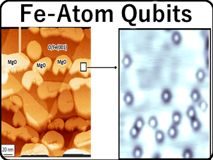
Stabilization of Isolated Fe Atoms on MgO/Fe(001) Insulating Surface via Critical Tunneling toward a Robust Quantum Spin Platform
Toyo Kazu Yamada, Nana K. M. Nazriq, Tada Kohei
Applied Surface Science Advances, 33, 100965 (2026).
DOI:10.1016/j.apsadv.2026.100965
accepted March 2, 2026, published April 2026.
[download: PDF]
[article 63]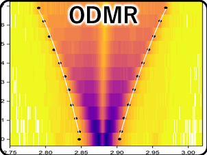
Magnetic Sensing and Imaging Using Nanodiamond NV Center Films and Microwave Integration into an STM Coplanar Waveguide Stage
Toyo Kazu Yamada, Achmad Yahiya Koki, Mai Niida
Japanese Journal of Applied Physics, 65, 050803 (2026). Special Issue: Scanning Probe Microscopy 2025 (SPM2025)
DOI: 10.35848/1347-4065/ae4a30
accepted February 24, 2026; published online March 16, 2026.
[download: PDF]
[article 62]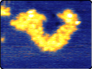
Spotlights
Thermally induced evolution of on-surface?synthesized crown ether polymers on Cu(111): transition from semiconductor chains to metallic nanoflakes
Toyo Kazu Yamada, Tomoya Kashiwagi, Masaki Horie
Japanese Journal of Applied Physics, 65, 05SP24 (2026). Special Issue: Scanning Probe Microscopy 2025 (SPM2025)
DOI:10.35848/1347-4065/ae498f
accepted February 23, 2026; published online March 12, 2026.
[download: PDF]
[report 26] 「量子ビット・量子センサーを実現する量子ナノ材料」企画趣旨
Quantum Nanomaterials for Qubits and Quantum Sensing: Concept Overview
山田豊和
「表面と真空」 Vacuum and Surface Science (第69巻 第2号)2026年2月10日印刷 2026年2月10日発行.
[download: PDF]
[report 25] 編集後記
編集後記
本年度のノーベル物理学賞「for the discovery of macroscopic quantum mechanical tunnelling and energy quantisation in an electric circuit」に象徴されるように、量子スピンの基礎研究は量子ビットなど多様な分野へ発展しています。
一方、室温・大気圧下で容易に利用できる量子コンピューターの実現には、依然として多様な量子材料の基礎研究開発が必要です。本特集では、表面や真空に関わる研究者の皆様に量子材料開発の現状と課題を共有し、新たな研究への一歩となることを願い企画しました。
山田豊和
「表面と真空」 Vacuum and Surface Science (第69巻 第2号)2026年2月10日印刷 2026年2月10日発行
[download: PDF]
[report 24] 「千葉大学 大学院工学研究院物質科学コース 山田豊和研究室の紹介」
山田豊和
応用物理学会 薄膜・表面物理分科会 News Letter 193号 「談話室」(2025).
[download: PDF]
[article 61]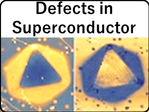
Editor's Suggestion
Visualization of defect-induced interband proximity effect at the nanoscale
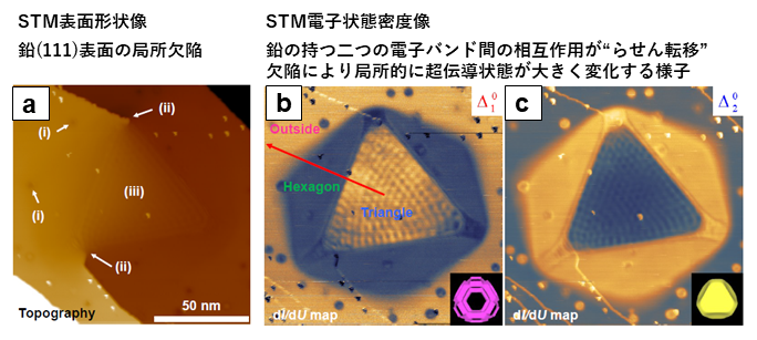
Thomas Gozlinski, Qili Li, Rolf Heid, Oleg Kurnosikov, Alexander Haas, Ryohei Nemoto, Toyo Kazu Yamada, Jorg Schmalian and Wulf Wulfhekel
Physical Review Letters 136, 056401 (2026).
DOI: 10.1103/4vhj-s1fq
accepted December 9, 2025 and publised February 4, 2026.
[download: PDF]
Press release: 鉛のもつ二つの超電導相を原子の積み重ねのずれで制御!
~超伝導内の積層欠陥がもたらす効果の可視化に成功~2次元薄膜で1次元電子ストライプ構造を創る!
Download, PDF.
【HP】
【PR TIMES】
【X】
【Facebook】
毎日新聞
[report 23] クラウンエーテル環状分子をホストとする磁性ナノ粒子・表面合成ポリマー・分子マシン薄膜の開発
山田豊和
分子研レターズ92, pp.56-57, September 2025, 共同利用研究ハイライト.
[download: PDF]
[article 60]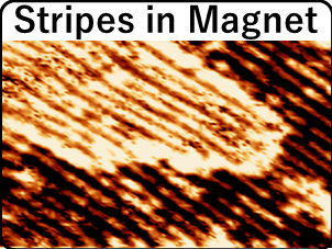 Emergence of Robust 1D Atomic and Electronic Textures in Mn Ultrathin Films via Antiferromagnet-Ferromagnet Interfaces
Eiichi Inami, Hiroki Hayashi, Peter Krueger, Toyo Kazu Yamada
Small 21, e04791 (2025).
DOI: 10.1002/smll.202504791
[download: PDF]
Press release: Japanese version
Download, PDF.
【HP】
【PR TIMES】
【X】
【Facebook】
日本経済新聞,
EE Times Japan
Nikkei Tech Foresight (日経テックフォアサイト)
[article 59]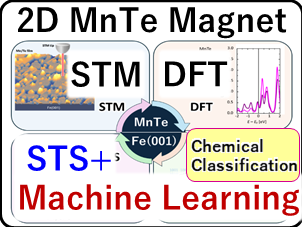 Tuning Epitaxial Growth of Atomically-Thin MnTe Films on Fe(001) for Creating van der Waals 2D Magnets
Haruto Seki, Kenji Nawa, Chiharu Mitsumata, Toyo Kazu Yamada
ACS Applied Nano Mater. 8, 31, 15662-15672 (2025).
DOI: 10.1021/acsanm.5c02678
[download: PDF]
[article 58] This article was selected as Nanoscale Horizons Most Popular 2025 Articles:
Nanoscale Horizons Most Popular 2025 Articles
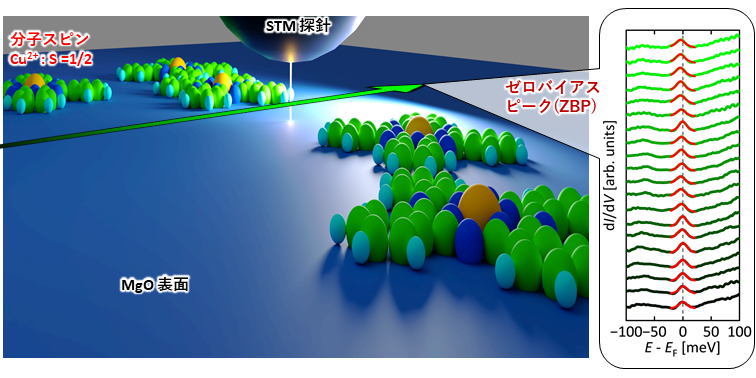
Emergence of a Zero-Bias Peak on the MgO/Fe(001) Surface Induced by the Adsorption of a Spin-1/2 Molecule
Kyosei Ishii, Nana K. M. Nazriq, Peter Kruger and Toyo Kazu Yamada
Nanoscale Horizons, 10, 2454-2464 (2025).
DOI: 10.1039/D5NH00192G
[download: PDF]
Press release: Japanese version
Download, PDF.
【PR TIMES】
【大学HP】
【X】
【Facebook】
日本経済新聞,
時事通信
Press release: English version
Download, PDF.
【EurekAlert英】
【EurekAlert日】
【CHIBADAI NEXT】
【大学HP】
【LinkedIn】
【Facebook】
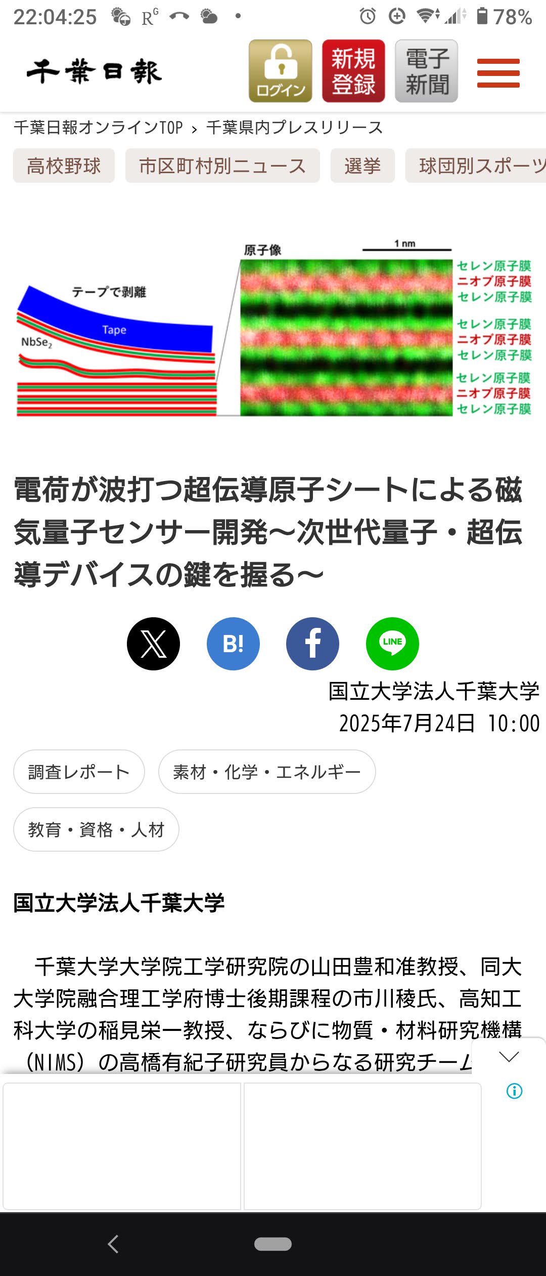
[article 57] Magnetic-Field Induced Dimensionality Switch of Charge Density Waves in Strained 2H-NbSe2 Surface
Ryo Ichikawa, Yukiko K. Takahashi, Eiichi Inami, and Toyo Kazu Yamada
npj 2D Materials and Applications, 9, 59 (2025).
DOI: https://doi.org/10.1038/s41699-025-00584-y
[download: PDF]
Press release: Japanese version
Download, PDF.
【PR TIMES】
【大学HP】
【X】
Online News
日本経済新聞,
千葉日報,
PEAKSMEDIA
EE Times Japan
Nikkei Tech Foresight (日経テックフォアサイト)
[article 56] STM imaging and electronic correlation in van der Waals ferromagnet Fe3GeTe2
Amir-Abbas Haghighirad, Ryo Ichikawa, Toshio Miyamachi, Haruki Ishii, Shun Akamatsu, Emiri Masui, Osamu Ishiyama, Hiroshi Iwayama, Eiken Nakamura, Toshihiko YOKOYAMA, Eiichi Inami and Toyokazu YAMADA
Japanese Journal of Applied Physics, 64. 040805 (2025).
DOI: 10.35848/1347-4065/adc7be
[download: PDF]
[review 24]【FLASH】
 フェロセンの「分子マシン」機能を発見!
山田豊和
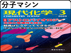
現代化学2025年3月号, 2025年2月18日出版 (JANコード 4910034870356).
[download: PDF]
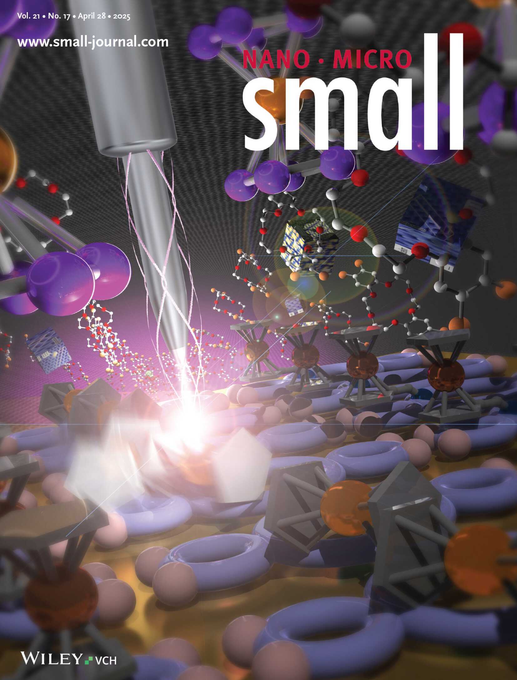
[article 55]
Cover image
Reversible Sliding Motion by Hole-Injection in Ammonium-Linked Ferrocene, Electronically Decoupled from Noble Metal Substrate by Crown-Ether Template Layer
Fumi Nishino, Peter Krueger, Chi-Hsien Wang, Ryohei Nemoto, Yu-Hsin Chang, Takuya Hosokai, Yuri Hasegawa, Keisuke Fukutani, Satoshi Kera, Masaki Horie and Toyo Kazu Yamada*
Small 2025, 21, 2408217
DOI: https://doi.org/10.1002/smll.202408217
[download: PDF]
 Supporting Information: PDF
Supporting Movie 1:gif movie
Supporting Movie 2:gif movie
Supporting Movie 3:gif movie
Press release: Japanese version
Download, PDF.
Press release: English version
Download, PDF
日本経済新聞社、毎日新聞社、日本の研究.com.
【EurekAlert】
【AlphaGalileo】
【CHIBADAI NEXT】
【大学HP】
【X】
【Facebook】
[review 23]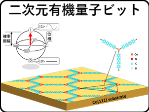 二次元有機量子ビットアレイ開発
Toward 2D Organic Quantum Bit Array
山田 豊和 Toyo Kazu Yamada
電気学会 電子図書館 (IEEJ Electronic Library) 論文 No. MAG24085 (pp.1-6)
[download: PDF]
[article 54]
Cover image
This article was selected as a part of the themed collections:
2025 Lunar New Year Collection
and
Nanoscale Horizons Most Popular 2024 Articles
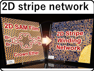 Designing 2D Stripe Winding Network Through Crown-Ether Intermediate Ullmann Coupling on Cu(111) Surface
Toyo Kazu Yamada, Ryohei Nemoto, Haruki Ishii, Fumi Nishino, Yu-Hsin Chang, Chi-Hsien Wang, Peter Krueger, Masaki Horie
Nanoscale Horizons, 2024, 9, 718-730.
.
DOI: 10.1039/d3nh00586k
[download: PDF]
Supporting Information: PDF
ニュースリリース PDF.
千葉大HP,
Chibadai Next,
PRtimes,
Twitter(X),
Facebook.
[article 53]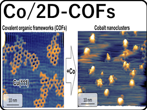 Growth of Transition-Metal Cobalt Nanoclusters on 2D Covalent Organic Frameworks
Toyo Kazu Yamada, Shingo Kanazawa, Keisuke Fukutani, Satoshi Kera
The Journal of Physical Chemistry C, 2024 128, 3, 1477-1486.
DOI: 10.1021/acs.jpcc.3c07435
[download: PDF]
Supporting Information: PDF
[article 52]
Cover image
 On-Surface Growth of Transition-Metal Cobalt Nanoclusters Using 2D Crown-Ether Array
Toyo Kazu Yamada, Ryohei Nemoto, Fumi Nishino, Takuya Hosokai, Chi-Hsien Wang, Masaki Horie, Yuri Hasegawa, Satoshi Kera, and Peter Krueger
Journal of Materials Chemistry C, 2024, 12, 874-883.
DOI: 10.1039/D3TC03339B
[download: PDF]
Supporting Information: PDF
ニュースリリース PDF.
[article 51]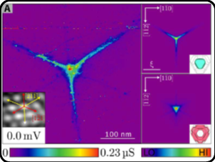 Band-resolved Caroli-de Gennes-Matricon states of multiple-flux-quanta vortices in a multiband
superconductor
Band-resolved Caroli-de Gennes-Matricon states of multiple-flux-quanta vortices in a multiband
superconductor
Thomas Gozlinski, Qili Li, Rolf Heid, Ryohei Nemoto, Roland Willa, Toyo Kazu Yamada, Joerg Schmalian, Wulf Wulfhekel
Sci. Adv. 9, eadh9163 (2023)
[download: PDF]
Supporting Materials: PDF
Data S1: HTML
Data S2: HTML
Data S3: HTML
Data S4: HTML
Data S5: HTML
Data S6: HTML
ニュースリリース PDF
:読売オンライン(PR times),
EE times,
日本物理学会HP,
マイナビニュース,
産経ニュース,
YouTube動画での紹介1,
YouTube動画での紹介2
.
[review 22]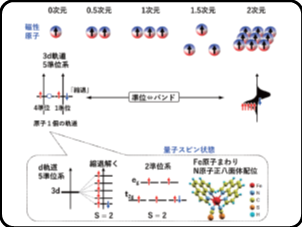 スピン偏極STMによる表面磁区観察から量子磁石計測へ
Spin-polarized STM study from surface magnetic imaging to quantum magnet measuring
山田 豊和 Toyo Kazu Yamada
野口研究所「時報」66号 公益財団法人野口研究所
[download: PDF]
[report 22]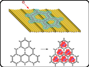 真空表面合成法による有機分子二次元ハニカム格子で実現する超高密度磁気記憶素子
山田 豊和
松籟科学技術振興財団 研究報告書第35集
[download: PDF]
[review 21]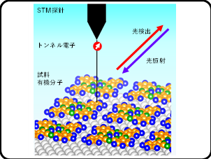 表面場を用いた新たな低次元分子磁性体の開発
山田 豊和
M&BE研究会「次世代に向けた有機分子・バイオエレクトロニクス最新研究」Vol.34 No.2(2023.6刊行)
M&BE. vol.34 No.2, pp.56-59 (2023).
[download: PDF]
[review 20]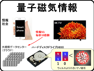 磁石がスマホ情報を保存している:古典磁石から量子磁石へ
材料の科学と工学に関わる新しい教育方法
【REVIEW】Magnetic Data Storage: from Classical to Quantum Magnets
山田 豊和, Toyo Kazu Yamada
「材料の科学と工学」Vol.60 No.2(2023.4.20刊行)
Materials Science and Technology of Japan(Mater. Sci. Tech. Jpn.) (2023.4.20).
[download: PDF]
[article 50]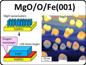 Improving MgO/Fe Insulator-Metal Interface Structure through Oxygen-Precoating of Fe(001)
Nana K. M. Nazriq, Peter Krueger, Toyo Kazu Yamada
Applied Surface Science 618, 156628 (2023) .
DOI: 10.1016/j.apsusc.2023.156628
[download: PDF]
Supplementary Information: PDF
[article 49]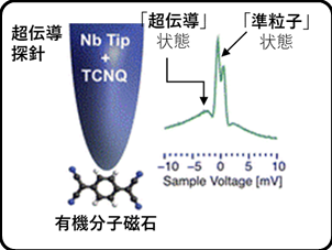 Switchable molecular functionalization of an STM tip: from a Yu-Shiba-Rusinov Tip to a Kondo tip
Cosme G. Ayani, Fabian Calleja, Ivan M. Ibarburu, Pablo Casado Aguilar, Nana K. M. Nazriq, Toyo K. Yamada, Manuela Garnica, Amadeo L. Vazquez de Parga and Rodolfo Miranda
Nanoscale 14, 15111-15118 (2022) .
DOI: 10.1039/D1NR08227B
[download: PDF]
Supplementary Information: PDF
ニュースリリース PDF
:HP, PR Times, Twitter, Facebook, 千葉日報.
[report 21]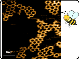 【Report, 報告書】
【助成38-12】超高密度2次元鉄ナノ磁石ハニカム規則配列作製による超省エネ電界書き込み制御型・磁気記憶素子の開発
【Report, 報告書】
【助成38-12】超高密度2次元鉄ナノ磁石ハニカム規則配列作製による超省エネ電界書き込み制御型・磁気記憶素子の開発
山田豊和
Annual Report of The Casion Science Promotion Foundation, pp.26-27 (2022).
[download: PDF]
[book 9] 朝倉書店|図説 表面分析ハンドブック, 日本表面真空学会 編
26.5 スピン偏極走査トンネル顕微鏡, Spin-polarized STM (SP-STM)
山田豊和 (Toyo Kazu Yamada)
B5/576ページ/2021年06月01日 ISBN978-4-254-20170-3 C3050
定価19,800円(本体18,000円+税)
[download: PDF]
[article 48]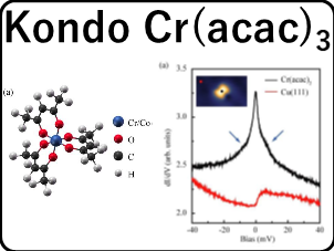 Interplay between point symmetry, oxidation state, and the Kondo effect in 3d transition metal acetylacetonate molecules on Cu(111)
Hongyan Chen, Timo Frauhammer, Satoru Sasaki, Toyo Kazu Yamada, and Wulf Wulfhekel
Physical Review B 103, 085423 (2021).
DOI: 10.1103/PhysRevB.103.085423
[download: PDF]
[article 47]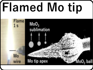 Oxidative Vaporization Etching for Molybdenum Tip Formation in Air
Yuto Goto, Rie Suizu, Yutaka Noguchi, and Toyo Kazu Yamada
Applied Surface Science 542, 148642 (2021).
DOI: 10.1016/j.apsusc.2020.148642
[download: PDF],
Supplementary Information: PDF
Supporting Movie of the Mo-tip Flame Etching
mp4 movie
[article 46]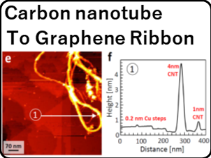 STM/STS計測によるCu(111)上に超高真空中で吸着したウェットカーボンナノチューブのアンジップ化検証
Unzipping Process of Wet Carbon NanotubesAdsorbedon Cu(111)in Ultra-High Vacuum:an STM / STSstudy
後藤悠斗, 安藤紗絵子, 角川佳樹, 高原茂, 山田豊和 (Yuto Goto, Saeko Ando, Keiju Kakugawa, Shigeru Takahara and Toyo Kazu Yamada)
表面と真空 64 (No.1) pp.40-46 (2021).
https://doi.org/10.1380/vss.64.40
[download: PDF]
[article 45] クラウンエーテル環状分子(7×4)配列へのコバルト単原子層の室温吸着:超高真空STM・UPS研究
Room-Temperature Deposition of Cobalt Monolayer on (7×4) Crown-Ether Ring Molecular Array: Ultra-High Vacuum STM and UPS Study
根本諒平・Peter Krueger・細貝拓也・堀江正樹・解良聡・山田豊和 (Ryohei Nemoto, Peter Krueger, Takuya Hosokai, Masaki Horie, Satoshi Kera and Toyo Kazu Yamada)
表面と真空 63 (No.9) pp.465-469 (2020).
https://doi.org/10.1380/vss.63.465
[download: PDF]
[article 44]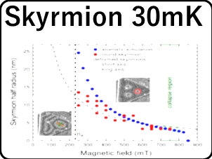 Instability of skyrmions in magnetic field
Loic Mougel, Patrick M. Buhl, Ryohei Nemoto, Timofey Balashov, Marie Herve, Julian Skolaut, Toyo Kazu Yamada, Bertrand Dupe, and Wulf Wulfhekel
Applied Physics Letters 116, 262406 (2020).
DOI: 10.1063/5.0013488.
[download: PDF]
[article 43]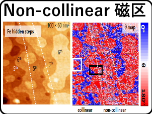 強磁性Fe(001)上のMn(001)超薄膜層間反強磁性への界面乱れによるノンコリニア磁気結合の発現:スピン偏極STM研究
Spin-Polarized Scanning Tunneling Microscopy Study of Non-Collinear Magnetic Coupling in Layerwise Antiferromagnetic Mn(001) Ultra-Thin Films on Fe(001) due to Interface Roughening
小菅 裕太郎、山田 豊和* (Yutaro Kosuge and Toyo Kazu Yamada*)
表面と真空 63 (No.9) pp.459-464 (2020).
https://doi.org/10.1380/vss.63.459
[download: PDF]
[review 19] 【Flash】 金属表面上で動く分子
現代化学 (Chemistry Today), Vol.591 No.6, pp.12-13 (2020), FLASH.
[download: PDF]
[article 42] 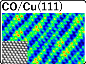 Carbon Monoxide Stripe Motion Driven by Correlated Lateral Hopping in 1.4 × 1.4 Monolayer Phase on Cu(111)
Nana K. M. Nazriq, Peter Krueger, and Toyo Kazu Yamada
The Journal of Physical Chemistry Letters 11, 1753-1761 (2020).
[download: PDF, Supplementary Information]
Supporting Movies: CO hopping
Movie1,
Movie2,
Movie3,
Movie4,
Movie5,
プレスリリース(PDF)。
日刊産業新聞(2020.3.23, 13面・非鉄)。
web release (WEBリリース)。
web 1。
web 2。
web 3。
[report 20]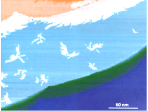 雪山へ舞う白鳥、安藤紗絵子, 根本諒平, 山田 豊和
応用物理学会誌, Science As Art, Vol.89 No.2, pp.63 (2020).
[download: PDF]
https://doi.org/10.11470/oubutsu.89.2_63
[article 41]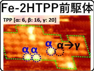 Direct Imaging of Precursor Adcomplex States during Cryogenic-Temperature On-Surface Metalation: Scanning Tunneling Microscopy Study on Porphyrin Array with Fe Adsorption at 78.5 K
F
Eiichi Inami, Masataka Yamaguchi, Ryohei Nemoto, Hideki Yorimitsu, Peter Krueger,
and Toyo Kazu Yamada
The Journal of Physical Chemistry C 124, 3621-3631 (2020).
[download: PDF, Supplementary Information]
[report 19] 超伝導基板上でのSTM磁性原子操作によりマヨラナ粒子の発現メカニズム解明,
Annual Report of The Murata Science Foundation, No.33, pp.480-488 (2019).
超伝導基板上でのSTM磁性原子操作によりマヨラナ粒子の発現メカニズム解明,
Annual Report of The Murata Science Foundation, No.33, pp.480-488 (2019).
[download: PDF]
[review 18]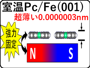 《次世代市場トレンド≫次世代先端デバイス動向(7)有機デバイス
~有機ELデバイスなどとして既に実用化されているが、さらに、高度な機能を発揮するものを創出する試みが精力的に進められている!~ (株式会社 矢野経済研究所 ヤノ イー プラス編集部). 5. 有機デバイスに関連する企業・研究機関の取組動向, 5-3. 国立大学法人 千葉大学 (山田 豊和)
《次世代市場トレンド≫次世代先端デバイス動向(7)有機デバイス
~有機ELデバイスなどとして既に実用化されているが、さらに、高度な機能を発揮するものを創出する試みが精力的に進められている!~ (株式会社 矢野経済研究所 ヤノ イー プラス編集部). 5. 有機デバイスに関連する企業・研究機関の取組動向, 5-3. 国立大学法人 千葉大学 (山田 豊和)
Yano E plus, No.140, pp.45-48 (2019). 2019年11月15日発行
[download: PDF]
[report 19] カブトムシの幼虫、ナズリク ナナ、山田 豊和
応用物理学会誌, Science As Art, Vol.88 No.10, pp.641 (2019).
[download: PDF]
https://doi.org/10.11470/oubutsu.88.10_641
[article 40]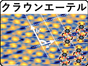 Well-Ordered Monolayer Growth of Crown-Ether Ring Molecules on Cu(111) in Ultra-High Vacuum: A STM, UPS, and DFT Study
Ryohei Nemoto, Peter Krueger, Ayu Novita Putri Hartini, Takuya Hosokai,
Masaki Horie, Satoshi Kera, and Toyo Kazu Yamada
The Journal of Physical Chemistry C 123, 18939-18950 (2019).
[download: PDF, Supplementary Information]
[article 39]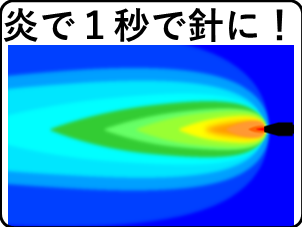 Fabrication of tungsten tip probes within 3 s by using flame etching
Takayuki Yamaguchi, Eiichi Inami, Yuto Goto, Yuta Sakai, Satoru Sasaki, Teruaki Ohno, and Toyo Kazu Yamada
Review of Scientific Instruments 90, 063701 (2019). (8 pages)
[download: PDF, Supplementary Information]
Movie: Flame Etching mp4 file movie
[report 18] 「JSPSフォトコンテスト」第13回応用物理学会フォトコンテスト作品, 2019年春季.
安藤紗絵子、根本諒平、山田豊和,
「雪山へ舞う白鳥」
[report 17]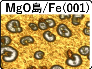 「JSPSフォトコンテスト」第13回応用物理学会フォトコンテスト作品, 2019年春季.
Nana K. M. Nazriq, 山田豊和,
「カブトムシの幼虫」
[article 38]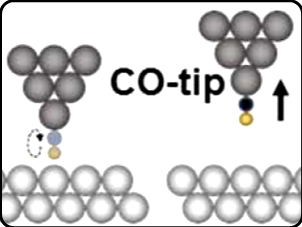 CO-tip manipulation using repulsive interactions
Nana K. M. Nazriq, Emi Minamitani, and Toyo Kazu Yamada
Nanotechnology 29, 495701 (2018).
[download: PDF, Supplementary Information]
[report 16]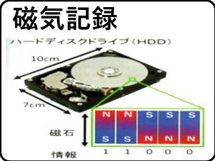 室温でも超安定!「世界最薄」有機分子膜を実現~磁石のパワーで分子膜を強力固定~
山田豊和,
千葉大学環境報告書, pp.18 (2018) 発行日2018.8.31.
[report 15] 原子欠陥制御による電界駆動Fe/MgO磁気デバイスの創成
山田豊和,
材料科学研究助成研究成果報告(公益財団法人 日立金属・材料科学財団), 第31集, pp.24-27 (2018).
[review 17]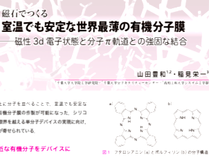 磁石でつくる室温でも安定な世界最薄の有機分子膜─磁性3d電子状態と分子π軌道との強固な結合 山田豊和, 稲見栄一
月刊「化学」 Vol. 73, No. 8, pp.44-48 (2018).
[download: PDF]
[patent 1] 【特許】山田豊和、稲見栄一, 発明の名称:薄膜形成方法及び記憶素子
出願日:平成30年6月5日, 出願番号:特願2018-107375, 特開2019-210511
[download: PDF]
[article 37]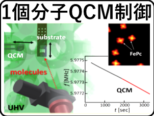 Controlled Deposition Number of Organic Molecules Using Quartz
Crystal Microbalance Evaluated by Scanning Tunneling Microscopy
Single-Molecule-Counting
Controlled Deposition Number of Organic Molecules Using Quartz
Crystal Microbalance Evaluated by Scanning Tunneling Microscopy
Single-Molecule-Counting
Eiichi Inami, Masataka Yamaguchi, Takayuki Yamaguchi, Mikio Shimasaki, and Toyo Kazu Yamada
Analytical Chemistry 90, pp. 8954-8959 (2018).
[download: PDF, Supplementary Information]
3D illustration by Dr. Inami
[article 36]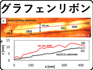 Energy Gap Opening by Crossing Drop Cast Single-Layer Graphene Nanoribbons
Toyo Kazu Yamada, Hideto Fukuda, Taizo Fujiwara, Polin Liu, Kohji Nakamura, Seiya Kasai,
Amadeo L. Vazquez de Parga and Hirofumi Tanaka
Nanotechnology 29, 315705 (2018).
[download: PDF, Supplementary Information]
[review 16]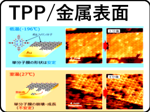 薄さは分子1個分!室温でも「超安定」な極薄有機分子膜‐磁気メモリの高密度化・省エネ化を促進, E. Inami and T. K. Yamada
academist Journal, 研究コラム, 2018年3月9日.
[download: PDF],
[article 35]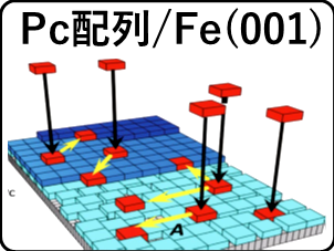 Room temperature stable film formation of π-conjugated organic molecules on 3d magnetic substrate
E. Inami, M. Shimasaki, H. Yorimitsu, and T. K. Yamada
Scientific Reports 8, 353 (2018)
[download: PDF, Supplementary Information]
プレスリリース。
日本経済新聞、他ネットニュース。
千葉日報(1面)。
日刊工業新聞。
日経産業新聞。
産業新聞。
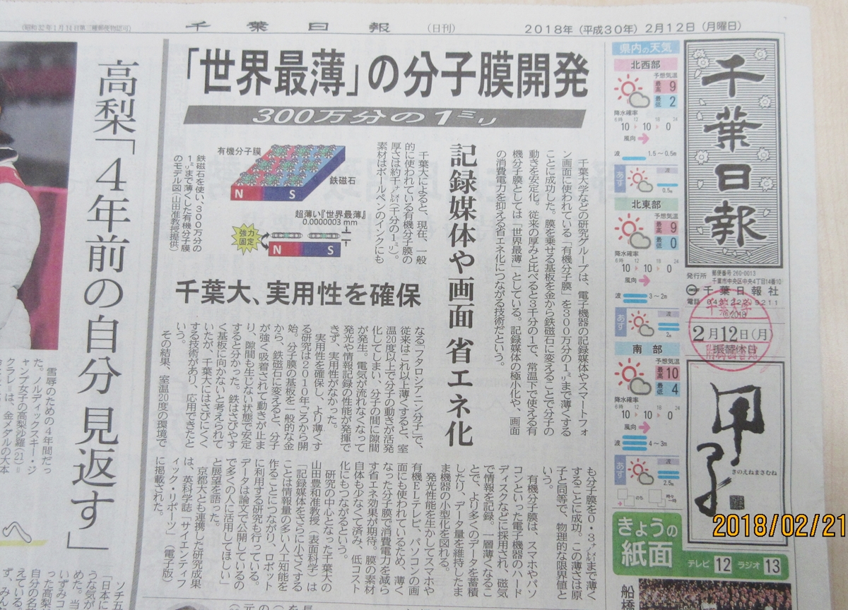
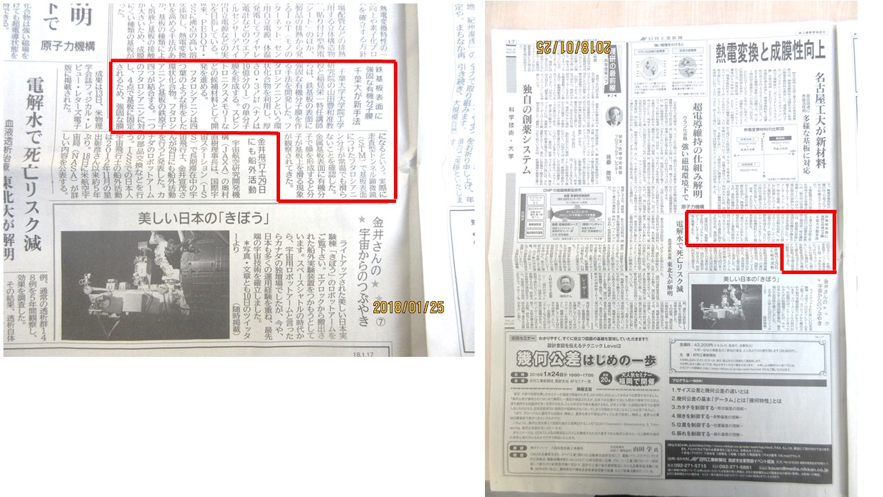
[report 14]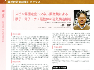 スピン偏極走査トンネル顕微鏡による原子・分子・ナノ磁性体の磁気構造解明,
山田豊和
科研費NEWS「最近の研究成果トピックス」, Vol.4, pp.10.
[book 8] Compendium of Surface and Interface Analysis, Chapter 103: Spin-polarized scanning tunneling microscopy (SP-STM)
Toyo Kazu Yamada
Springer, Singapore, DOI: 10.1007/978-981-10-6156-1
(日本表面科学会"表面分析図鑑"英語版), pp. 637-642, (2018).
[download: PDF]
[review 15]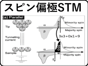 スピン偏極STMの発展の歴史と今後の課題,
山田豊和,
日本真空学会誌 (Journal of the Vacuum Society of Japan), 60巻, No.5, pp. 159-164, 2017年.
[download: PDF]
[book 7]  Molecular Architectonics
The Third Stage of Single Molecule Electronics
Spin polarization of single organic molecules: towards single molecular spintronics
T. K. Yamada
Springer, pp. 381-397, (2017). ISBN 978-3-319-57096-9, (eBook) DOI 10.1007/978-3-319-57096-9
[download: XPS]
[article 34]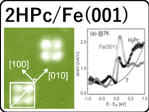 Role of π-d hybridization in 300-K organic-magnetic interface: metal-free phthalocyanine single molecules on bcc Fe(001)-whisker
T. K. Yamada, Y. Yamagishi, S. Nakashima, Y. Kitaoka, and K. Nakamura
Phys. Rev. B 94, 195437 (2016).
Selected as “Kaleidoscope”
[download: PDF]
[article 33]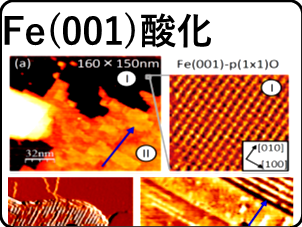 Temperature control of the growth of iron oxide nanoislands on Fe(001)
Toyo Kazu Yamada, Yuki Sakaguchi, Lukas Gerhard, and Wulf Wulfhekel
Japanese Journal of Applied Physics 55, 08NB14 (2016).
[download: PDF]
[article 32]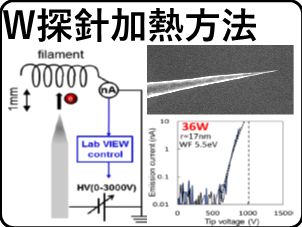 Electron-bombarded <110>-oriented tungsten tips for stable tunneling electron emission
T. K. Yamada, T. Abe, N. M. K. Nazriq, and T. Irisawa
Review of Scientific Instruments 87, 033703 (2016).
[download: PDF]
[report 13] 表面上の原子スピン (Atomic spins on surfaces, Andreas Heinrich, Physics Today)
山田豊和
パリティ, 31 (2016) 24-31.
[download: PDF]
[report 12] 極限スピン観察と制御:SP-STM (PDF 1.4MB)
山田豊和
日本磁気学会 第210回研究会資料「“スピン”の可視化とその操作」 (2016) 17-21.
[article 31]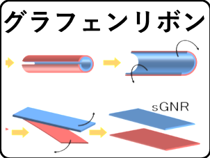 Method for Controlling Electrical Properties of Single-Layer Graphene Nanoribbons via Adsorbed Planar Molecular Nanoparticles,
Hirofumi Tanaka, Ryo Arima, Minoru Fukumori, Daisuke Tanaka, Ryota Negishi, Yoshihiro Kobayashi, Seiya Kasai, Toyo Kazu Yamada and Takuji Ogawa
Scientific Reports, 5 (2015), 12341.
[download: PDF, Supplementary Information]
プレスリリース:日刊工業新聞(紙面)。
日刊工業新聞(ネット)。
[review 14]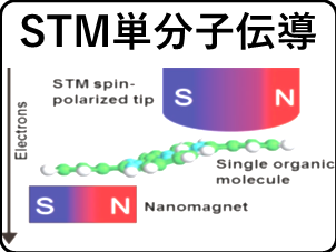 How to get molecular spin-polarization using spin-polarized STM,
T. K. Yamada,
How to get molecular spin-polarization using spin-polarized STM,
T. K. Yamada,
Journal of The Surface Science Society of Japan, 36 (2015) 375-381.
[download: PDF]
[book 6] Electronic processes in organic electronics
: Bridging electronic states and device properties
Chapter 18: Single molecular spintronics, T. K. Yamada
Springer, Tokyo、Springer Series in Materialsa Science 209, (2015) pp.403-416.
[report 11]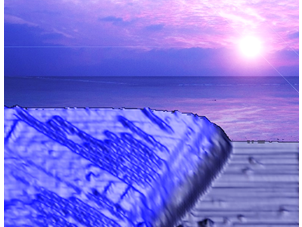 「JSPSフォトコンテスト」第62回応用物理学会春季学術講演会, 坂口雄基、山田豊和
「題名:酸化鉄原子層台地」
走査トンネル顕微鏡によるFe(001)-p(1x1)O原子テラス上に成長したマグネタイトテラスの原子形状像。2015.3.11-14.
[report 10]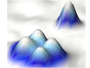 「JSPSフォトコンテスト」第62回応用物理学会春季学術講演会, 中島脩平、山田豊和
「題名:世界最小・雲の上の山」
極低温走査トンネル顕微鏡によるCu(111)原子テラス上に吸着した鉄の原子1個とフタロシアニン有機分子1個を観察した像。」
[report 9] 「JSPSフォトコンテスト」第62回応用物理学会春季学術講演会, 阿部巧、山田豊和
「題名:タングステン単結晶山」
単結晶化したタングステン線を化学エッチングして作成した針。
[article 30]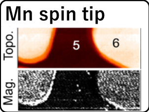 Room temperature spin-polarizations of Mn-based antiferromagnetic nanoelectrodes (Mn tip spin polarization)
T. K. Yamada and A. L. Vazquez de Parga
Appl. Phys. Lett. 105 (2014) pp.183109: 1-5.
[download: PDF]
[book 5] マイクロビームアナリシス・ハンドブック
第2.3.2章スピン偏極走査トンネル顕微鏡
山田豊和、オーム社、東京、pp.203-206, 2014年.
[download (50MB)]
[book 4] 強力永久磁石の開発と磁区観察先端技術
第1章スピン偏極STM開発技術、山田豊和、日本学術振興会産学協力研究委員会特別事業、日本学術振興会マイクロビームアナリシス第141委員会編纂、東京、pp.1-32, 2014年
[download! (43MB)]
[report 8] 応用物理学会誌、図解・学術講演会大分類 表面・薄膜分野 , 山田豊和
「スピン偏極走査トンネル顕微鏡(STM)による1nmサイズの単一有機分子を用いた世界最小・磁気抵抗センサーの実証実験。フタロシアニン分子を介する伝導を磁性探針とナノ磁石の磁気結合(平行・反平行)で制御。」 2014年8月号.
[report 7] 追悼: 溝口正先生を偲んで。
山田豊和
日本磁気学会誌まぐね, 9 (2014) 245.
[article 29]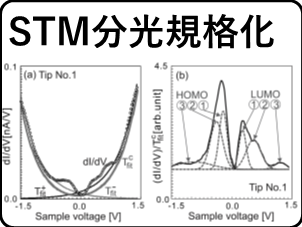 Recovery of nanomolecular electronic states from tunneling spectroscopy: LDOS of low-dimensional phthalocyanine molecular structures on Cu(111),
Y. Yamagishi, S. Nakashima, K. Oiso and T. K. Yamada,
Nanotechnology 24 (2013) 395704 (11pp).
[download: PDF]
[article 28]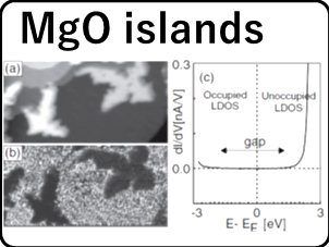 How contacting electrodes affect single π-conjugated molecular electronic states: LDOS of phthalocyanine nano molecules on MgO(001), Cu(111), Ag(001), Fe(001) and Mn(001) [Selected Topics in Applied Physics (Nano Electronics and Devices)]
Shuhei Nakashima, Yuhei Yamagishi, Kenji Oiso, Toyo Kazu Yamada,
Jpn. J. Appl. Phys. 52 (2013) 110115.
[download: PDF]
[review 13]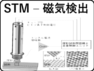 スピン偏極走査トンネル顕微鏡:ナノ材料の原子スケール磁気イメージング
山田豊和
日本顕微鏡学会誌, 48 (2013) 20-25.
[download: PDF]
[review 12]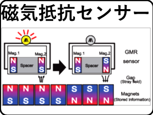 単一ナノ分子・磁気抵抗素子~スピン偏極STMによる単一分子電子スピン伝導測定~
山田豊和
表面科学, 34 (2013) 443-448.
[download: PDF]
[report 6]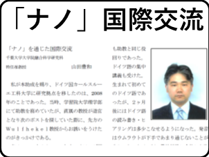 「ナノ」を通じた国際交流。
山田豊和
公益財団法人山田科学振興財団 財団ニュース平成25年度第1号、pp.18, 2013年
[article 27]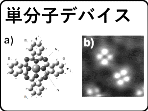 Spintronics with single molecules,
W. Wulfhekel, T. Miyamachi, S. Schmaus, T.K. Yamada, A. F. Takacs, A. Bagrets, F. Evers, T. Balashov, M. Gruber, V. Davesne, M. Bowen, and E. Beaurepaire
IEEE NANO proceedings, 2012 12th IEEE Internationa; Conference on Nanotechnology, (2012) 957-961.
[download: PDF]
[article 26]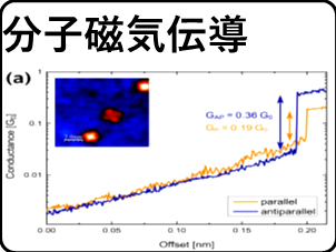 Single molecule magnetoresistance with combined antiferromagnetic and ferromagnetic electrodes,
A. Bagrets, S. Schmaus, A. Jaafar, D. Kramczynski, T.K. Yamada, M. Alouani, W. Wulfhekel, and F. Evers,
Nano Letters, 12, (2012) 5131-5136.
[download: PDF, Supplementary Information]
[article 25]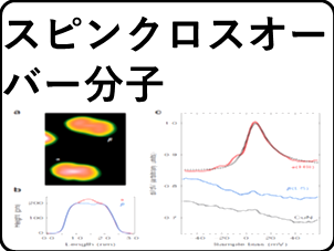 Robust spin crossover and memristance across a single molecule,
T. Miyamachi, M. Gruber, V. Davesne, M. Bowen, S. Boukari, F. Scheurer, G. Rogez, T. K. Yamada, P. Phresser, E. Beaurepaire, and W. Wulfhekel,
Nature Communications, 3, (2012) 938.
[download: PDF]
プレスリリース。
NHK news (pictures)。
NHK news (movie: 32MB)。
千葉日報、産経新聞、読売新聞、毎日新聞。
[review 11]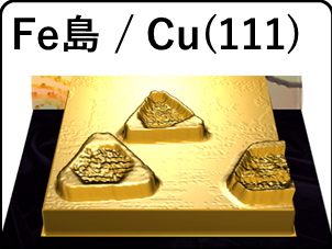 Electric Field Control of Fe Nano Magnets,
T. K. Yamada, L. Gerhard, R. J. H. Wesselink, A. Ernst, and Wulf Wulfhekel,
J. Magn. Soc. Jpn., 36, (2012) 100-103.
[download: PDF]
[review 10]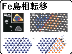 電界による鉄ナノ磁石制御:金属表面での磁気電気結合
山田豊和
日本金属学会誌まてりあ, 51 (2012) 475-479.
[download: PDF]
[review 9]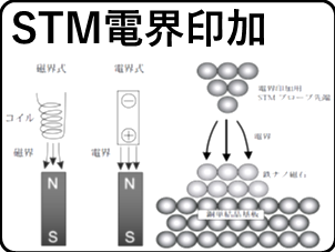 ~従来の100倍容量の記録を可能にする~新しい鉄ナノ記録材料
山田豊和
Material Stage (月刊 マテリアルステージ), 12 (2012) 57-60.
[report 5] 留学経験を土台に世界を舞台に研究
山田豊和
日経BPムック・学習院大学理学部広報誌, pp.26-27, 2012年.
[report 4]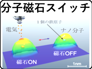 1個の鉄原子で情報記録に成功!~世界最小・ナノ分子磁気メモリ~
山田豊和
千葉大学「研究成果の見える化」最近の革新的な研究成果, pp.2, 2012年.
[report 3] 1個の鉄原子で情報記録に成功!~世界最小・ナノ分子磁気メモリ~
山田豊和
千葉大学「千葉大プレス」, pp.15, 2012年.
[report 2] 世界最小・ナノ分子磁気メモリ
山田豊和
千葉大学「Chiba University Handbook」, pp.12, 2012年.
[article 24]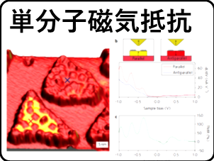 Giant magnetoresistance through a single molecule,
S. Schmaus, A. Bagrets, Y. Nahas, T.K. Yamada, A. Bork, F. Evers, and W. Wulfhekel,
Nature Nanotechnology, 6, (2011) 185-189.
[download: PDF, Supplementary Information]
プレスリリース(パワポ)。
プレスリリース(用紙)。
プレスリリース(記者会見)。
新聞(紙面):読売新聞、毎日新聞、千葉日報。
R25。
NatureJapan。
ジャパンナレッジ。
千葉大学・千葉理数教育高大連携ニュース No.42。
文教ニュース。
[article 23]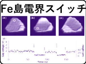 Electrical control of the magnetic state of Fe,
L. Gerhard, T. K. Yamada, T. Balashov, A. F. Takacs, M. Daena, S. Ostanin, A. Ernst, I. Mertig, and W. Wulfhekel,
IEEE Transactions on Magnetics, 47, (2011) 1619-1622.
[download: PDF]
[review 8]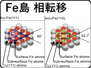 Electric field control of Fe nano magnets: towards metallic non-volatile data-storage devices,
Toyo Kazu Yamada, Lukas Gerhard, Timofey Balashov, Albert F. Takacs, Rien J. H. Wesselink, and Wulf Wulfhekel,
Japanese Journal of Applied Physics, 50 (2011) 08LA03: 1-5.
[download: PDF]
[review 7] STMが切り拓く新たなスピンデバイスの創成,
山田豊和
日本磁気学会誌まぐね, 6 (2011) 333-341.
[review 6] 【Editor’s Choice】電界による鉄ナノ磁石制御:金属表面での磁気電気結合の発見
山田豊和
表面科学, 32 (2011) 361-367.
[download: PDF]
[article 22] Magneto-electric coupling at metal surfaces,
L. Gerhard, T.K. Yamada, T. Balashov, A.F. Takacs, M. Daena, S. Ostanin, A. Ernst, I. Mertig, and W. Wulfhekel,
Nature Nanotechnology, 5, (2010) 792-797.
[download: PDF, Supplementary Information]
News & views: Making metallic memories by Dr. R. Ramesh.
[download: PDF]
記者会見。
プレスリリース。
毎日新聞、朝日新聞、千葉日報、日本経済新聞。
[book 3] 磁気イメージングハンドブック, 日本磁気学会編,
編集幹事:大島則和、小野寛太、笹田一郎、三俣千春、山田豊和、
山田豊和, 第1章. (2010) 15-44.
共立出版、東京、2010年9月15日、ISBN 978-4-320-03468-6
2015年日本磁気学会 出版賞
[article 21] Spin polarization vectors of field emitted electrons from apexes of Fe-coated W tips,
T. Irisawa, T. K. Yamada, and T. Mizoguchi,
New Journal of Physics, 11, (2009) 113031.
[download: PDF]
[article 20]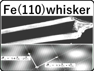 Surface reconstruction of clean bcc-Fe{110}: A quasi-hexagonal top-layer with periodic height modulation,
T. K. Yamada, H. Tamura, M. Shishido, T. Irisawa, and T. Mizoguchi,
Surface Science, 603, (2009) 315-319.
[download: PDF]
[article 19] Requirement of Ala residues at g position in heptad sequence of α-helix-forming peptide for formation of fibrous structure,
G. Aoki, T. K. Yamada, M. Arii, S. Kojima and T. Mizoguchi,
Journal of Biochemistry, 144, (2008) 15-19.
[download: PDF]
[article 18]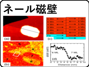 Spin configuration in a frustrated ferromagnetic/antiferromagnetic thin-film system,
T. K. Yamada, E. Martinez, A. Vega, R. Robles, D. Stoeffler, A. L. Vazqeuz de Parga, T. Mizoguchi and H. van Kempen,
Nanotechnology, 18 (2007) 235702: 1-6.
[download: PDF]
[review 5]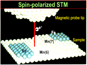 Spin-Polarized Scanning Tunneling Microscopy (cover image (表紙))
T. K. Yamada and T. Mizoguchi
The Physical Society of Japan, 62巻, No.7, pp.499-508, 2007年.
[download: PDF]
[review 4]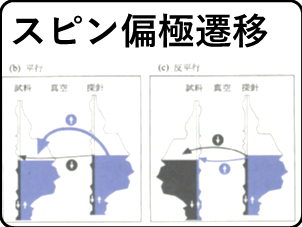 Spin-Polarized STM/STS: An Ultimate Experiment in Magnetism
T. K. Yamada and T. Mizoguchi
Solid State Physics, 42 (2007) 749-756.
[download: PDF]
[article 17] Enormous electron emission from polygonal W tip,
T. Irisawa, T. K. Yamada, and T. Mizoguchi,
6th International Symposium on Atomic Level Characterizations for New Materials and Devices 2007 (ALC07) Proceedings: JSPS1441 Committee Activity Report (2007).
[report 3] Spin-Polarized Scanning Tunneling Microscopy / Spectroscopy,
T. K. Yamada,
Report of The Magnetics Society of Japan Symposium, 155 (2007) 41-46.
[report 2] Study of magnetic interaction between ferromagnetic and anti-ferromagnetic layers by means of spin-polarized scanning tunneling spectroscopy: Fe/Mn/Fe(001)-multilayers,
T. K. Yamada, and T. Mizoguchi,
Report of The Magnetics Society of Japan Symposium, 140 (2007) 21-27.
[article 17]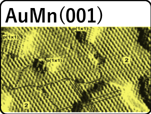 Study of c(2x2)-MnAu(100) layers on Mn(001) by means of scanning tunneling microscopy /spectroscopy,
T. K. Yamada, A. L. Vazqeuz de Parga, M. M. J. Bischoff, T. Mizoguchi and H. van Kempen,
Surface Science, 600 (2006) 1048-1053.
[download: PDF]
[article 16]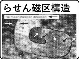 Evaluation of sample spin-polarization from spin-polarized scanning tunneling spectroscopy experiments,
T. K. Yamada, A. L. Vazquez de Parga, M. M. J. Bischoff, T. Mizoguchi, and H. van Kempen,
Microscopy Research and Technique, 66 (2005) 93-104.
[download: PDF]
[article 15]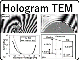 Characterization of Fe/W spin-polarized tips by means of holographic TEM and spin-polarized STS of optically pumped p-GaAs,
T. Matsuda, A. Tonomura, T. K. Yamada, D. Okuyama, N. Mizuno, A. L. Vazqeuz de Parga, H. van Kempen and T. Mizoguchi,
IEEE Transactions and Magnetics, 41 (2005) 3727-3729.
[download: PDF]
[review 3] Study of magnetic structure of manganese (001) atomic layers by means of spin-polarized scanning tunneling microscopy / spectroscopy having sub-nanometer scale magnetic resolution,
T. K. Yamada and T. Mizoguchi,
Materia Japan, 44, (2005) 975.
[download: PDF]
[article 14]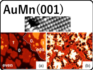 Spin-polarized scanning tunneling microscopy / spectroscopy study of MnAu(001) thin films,
T.K. Yamada, R. Robles, E. Martinez, M.M.J. Bischoff, A. Vega, A.L. Vazqeuz de Parga, T.Mizoguchi and H. van Kempen,
Physical Review B, 72 (2005) 014410: 1-4.
[download: PDF]
[review 2]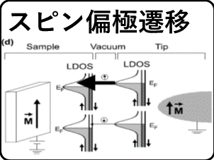 Spin-Polarized Scanning Tunneling Microscopy/Spectroscopy and Quantitative Analysis studied on Mn(001)
T. K. Yamada and T. Mizoguchi
Journal of The Surface Science Society of Japan, 26 (2005) 2-10.
[download: PDF]
[book 2]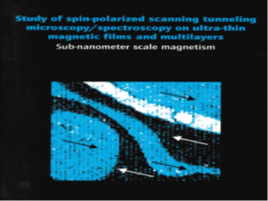 Study of spin-polarized scanning tunneling microscopy/spectroscopy on ultra-thin magnetic films and multilayers: sub-nanometer scale magnetism,
T. K. Yamada,
Radboud University Nijmegen, Ph.D thesis (2005) pp.1-193. ISBN90-9019035-X
[download: PDF (19MB)]
[article 13]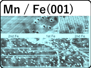 Study of Fe/Mn/Fe(001) multilayers by means of scanning tunneling microscopy/spectroscopy,
T. K. Yamada, M. M. J. Bischoff, A. L. Vazqeuz de Parga, T. Mizoguchi and H. van Kempen,
Surface Science, 558 (2004) 201-210.
[download: PDF]
[book 1] Sub-Nanometer Scale Mgnetism of Ultra-Thin Manganese Films on Fe(001) studied by means of Spin-Polarized Scanning Tunneling Microscopy/Spectroscopy,
T. K. Yamada,
Gakushuin University, Ph.D thesis (2004) pp.1-113.
[download: PDF (30MB)]
[report 1] Introduction of Basic Magnetism through Experiments V,
T. Mizoguchi and T. K. Yamada,
Journal of the Magnetics Society of Japan, 28 (2004) 1142-1149.
[article 12]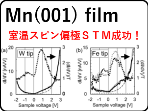 Observation of spin-polarized surface states on ultrathin bct Mn(001) films by spin-polarized scanning tunneling spectroscopy,
T. K. Yamada, M. M. J. Bischoff, G. M. M. Heijnen, T. Mizoguchi, and H. van Kempen,
Physical Review Letters, 90 (2003) 056803: 1-4.
[download: PDF]
[article 11]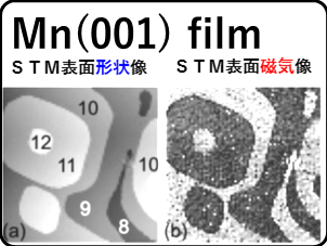 Origin of magnetic contrast in spin-polarized scanning tunneling spectroscopy: experiments on ultra-thin Mn films
T. K. Yamada, M. M. J. Bishoff, G. M. M. Heijnen, T. Mizoguchi, and H. van Kempen,
Japanese Journal of Applied Physics, 42 (2003) 4688-4691.
[download: PDF]
[article 10]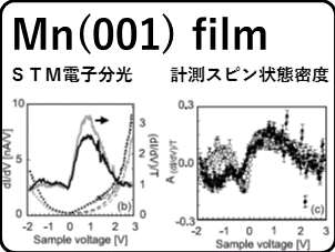 Data evaluation for spin-polarized scanning tunneling spectroscopy measurements,
T. K. Yamada, A. L. Vazquez de Parga, M. M. J. Bischoff, T. Mizoguchi, and H. van Kempen,
AIP Conf. Proc., 696 (2003) 608-614.
[download: PDF]
[article 9] Use of voltage pulses to detect spin-polarized tunneling (Cover image, 表紙)
T. K. Yamada, M. M. J. Bischoff, T. Mizoguchi, and H. van Kempen
Applied Physics Letters, 82 (2003) 1437-1439. (Cover image)
[download: PDF]
[review 1]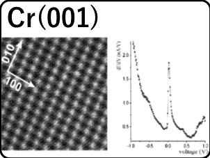 Scanning Tunneling Spectroscopy Study of Surface States of 3d Metals: Chemical Identification, Magnetic Contrast and Orbital Kondo Resonance State,
M. M. J. Bischoff, C. M. Fang, R. A. de Groot, G. M. M. Heijnen, M. I. Katsnelson, O. Yu. Kolesnychenko, R. de Kort, A. I. Lichtenstein, A. J. Quinn, A. L. Vazqeuz de Parga, T. K. Yamada and H. van Kempen,
Acta Physica Polonica A, 104 (2003) 231-243.
[download: PDF]
[article 8]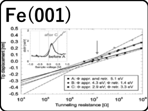 Local electronic structure of Fe(001) surfaces studied by scanning tunneling spectroscopy,
M. M. J. Bischoff, T. K. Yamada, C. M. Fang, R. A. de Groot and H. van Kempen,
Physical Review B, 68 (2003) 045422: 1-7.
[download: PDF]
[article 7]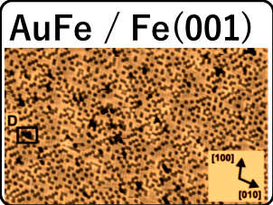 Analysis of the short-range order of the Au/Fe(001) surface alloy,
M. M. J. Bischoff, T. K. Yamada, and H. van Kempen
Physical Review B, 67 (2003) 165403: 1-7.
[download: PDF]
[article 6]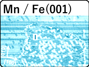 Scanning tunneling microscopy and spectroscopy study on the submonolayer growth of Mn on Fe(001)
M. M. J. Bischoff, T. Yamada, A. J. Quinn, and H. van Kempen
Surface Science, 501 (2002) 155-167.
[download: PDF]
[article 5]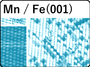 STM and STS study of ultrathin Mn layers on Fe(001),
T. K. Yamada, M. M. J. Bischoff, T. Mizoguchi, and H. van Kempen,
Surface Science, 516 (2002) 179-190.
[download: PDF]
[article 4] Photoemission and STM, STS Study of Cs/p-GaAs(110),
T. Yamada, J. Fujii, T. Mizoguchi
CP570, SPIN2000, 14th International Spin Physics Symposium, 908-911, (2001).
[article 3]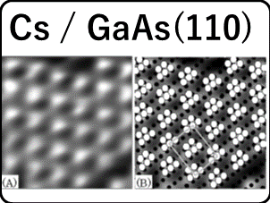 STM, STS, and Local Work Function Study of Cs/p-GaAs(110),
T. Yamada, J. Fujii, T. Mizoguchi,
Surface Science, 479 (2001) 33-42.
[download: PDF]
[article 2]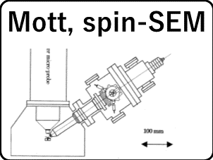 Polarization of Secondary Electrons from Clean and Oxygen-Chemisorbed Ni(110),
Y. Oshima, T. Yamada, J. Fujii, and T. Mizoguchi,
Trans. Magn. Soc. Japan, 1 (2001) 16-21.
[download: PDF]
[article 1]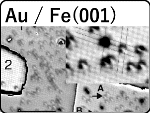 Direct observation of surface alloying and interface roughening: Growth of Au on Fe(001),
M. M. J. Bischoff, T. Yamada, A. J. Quinn, R. G. P. van der Kraan, and H. van Kempen,
Physical Review Letters, 87 (2001) 246102: 1-4.
[download: PDF]
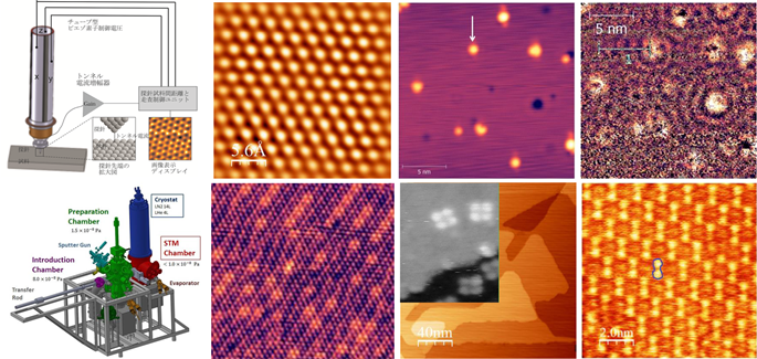
○写真・画像・文章の無断転載を禁止します.著作権は千葉大学山田豊和研究室にあります.
Toyo Kazu Yamada Lab.山田豊和研究室
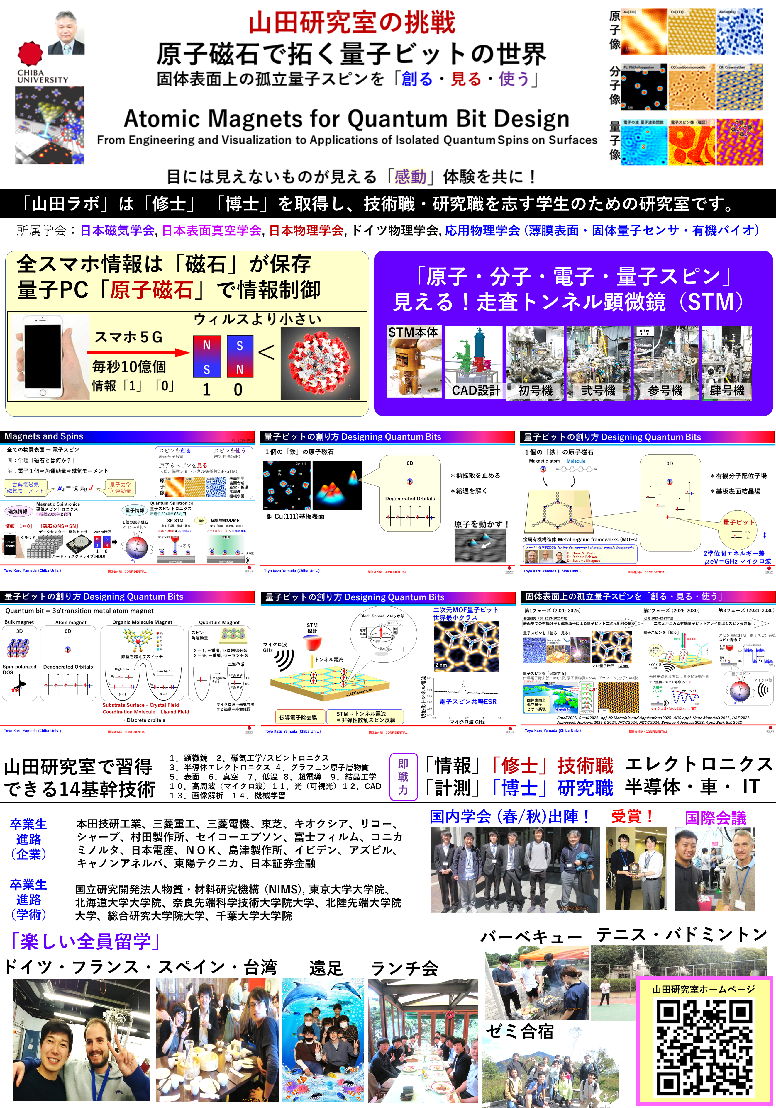 .
. Press Release
〒263-8522
1-33, Yayoi-chou, Inage-ku, Chiba-shi, Chiba, JAPAN
E-mail: toyoyamada[at]faculty.chiba-u.jp ([at]を@にしてください)
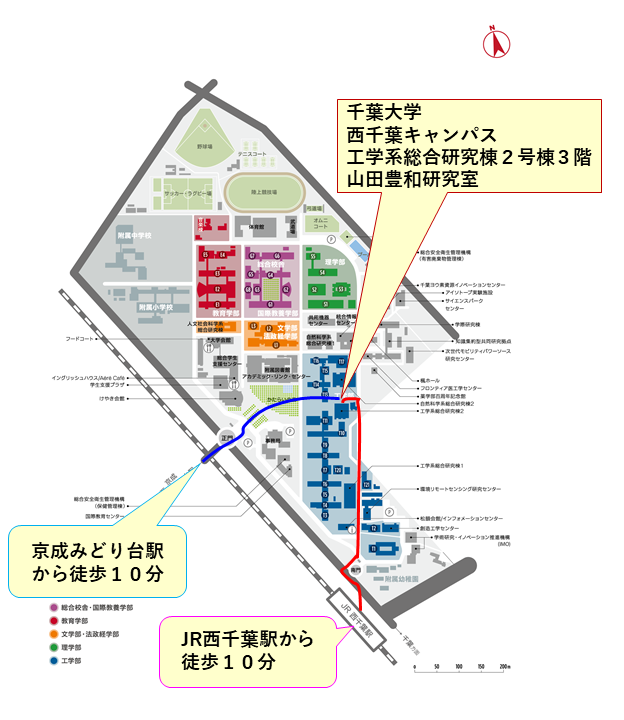
PhD Radbound University Nijmegen (The Netherlands, March 2005)
PhD (Science) Gakushuin University (Japan, March 2004)
Career, Awards, and Social Contributions
CHIBADAI NEXT.
ResearchMap.
Research Gate.
ORCID.
Publons (Web of Science).
Google Scholar.
N and S using 17 Iron Atoms
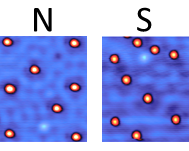
STM Atom Manipulation
STM Molecule Manipulation
Molecule Rotor !?
We are promoting our research with strong collaborations by many researchers.
Research Collaboration Network。
(1) Japan Society of Applied Physics (JSAP),
(2) The Physical Society of Japan (JPS),
(3) The Japan Society of Vacuum and Surface Science,
(4) The Magnetics Society of Japan (MSJ),
(5)The German Physical Society (DPG)
Lectures for Under Graduate School
(1) Physics in Surface Science. (2) Introductory Exercise of Materials Science. (3) Mechanics (Basic) 2. (4) Exercises on Mechanics (Basic) 2. (5) Laboratory Work in Materials Science IA. (6) Laboratory Work in Materials Science IIA. (7) Laboratory Work in Materials Science IIIA.
Lectures for Graduate School
(1) Science in Magnetic Materials. (2) Special Lecture on Advanced Science and Engineering IIa. (3) Advanced Seminar I. (4) Graduate Research I.
All our lab. members have studied abroad. !
Hiiragi-kai 柊会(ひいらぎ会)
OB/OG meeting room.
If you need contact, please send an email to Dr. Toyo Yamada or the secretary-general: Ms. Saeko Ando (OG).
山田ラボ「装置」写真
自作超高真空STM装置CAD図面
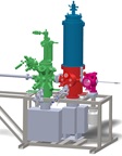
自作STM本体
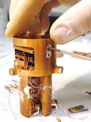
「初号機」自作・超高真空STM装置
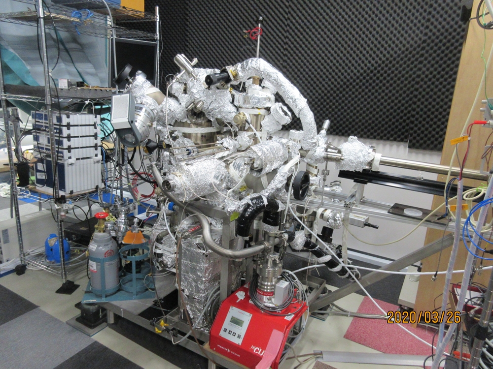
「弐号機」自作・超高真空STM装置
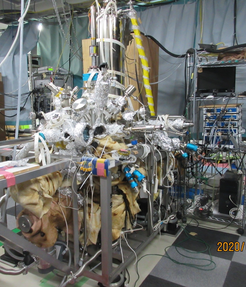
「参号機」自作・超高真空STM装置

「四号機」自作・超高真空STM装置
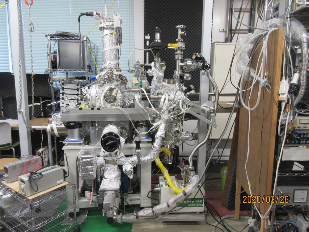
「製膜装置」自作・SEMと伝導計測付属
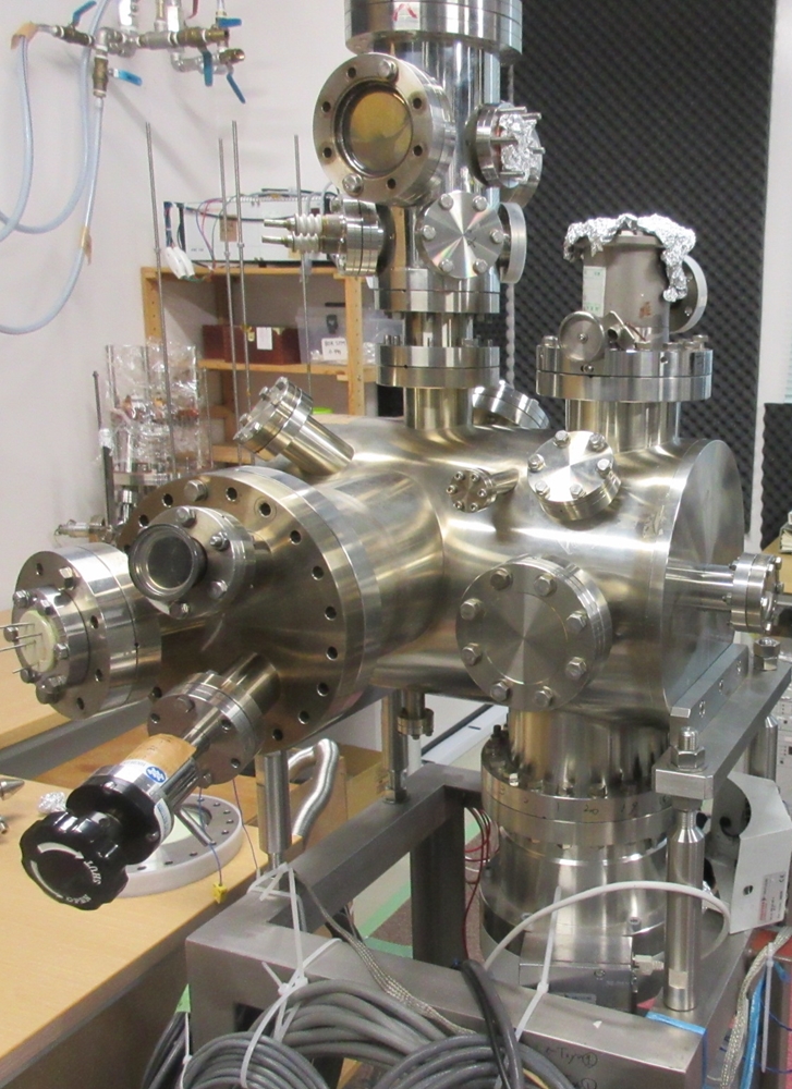
「FEM」自作・電子分光とMott検出器付属装置

「超電導コイル」Spemag-7T磁気光学と磁気伝導計測装置
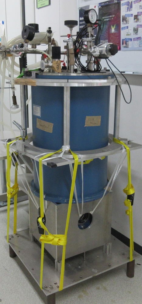
「AFM/STM」JEOL4200装置
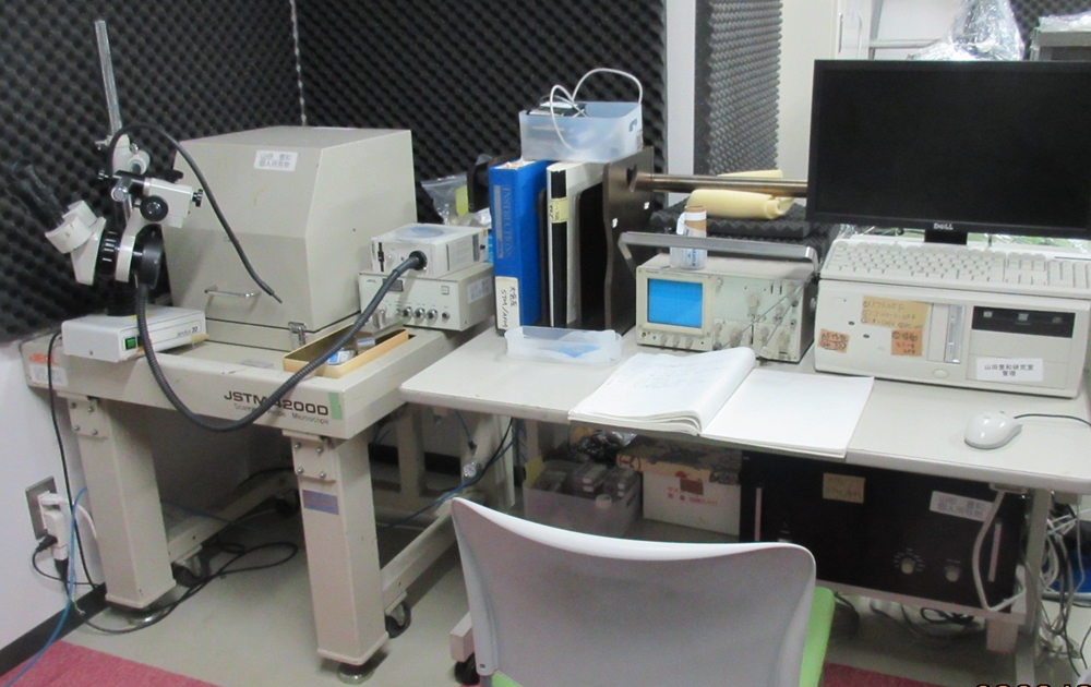
「Tiny-SEM」テクネックス工房社装置
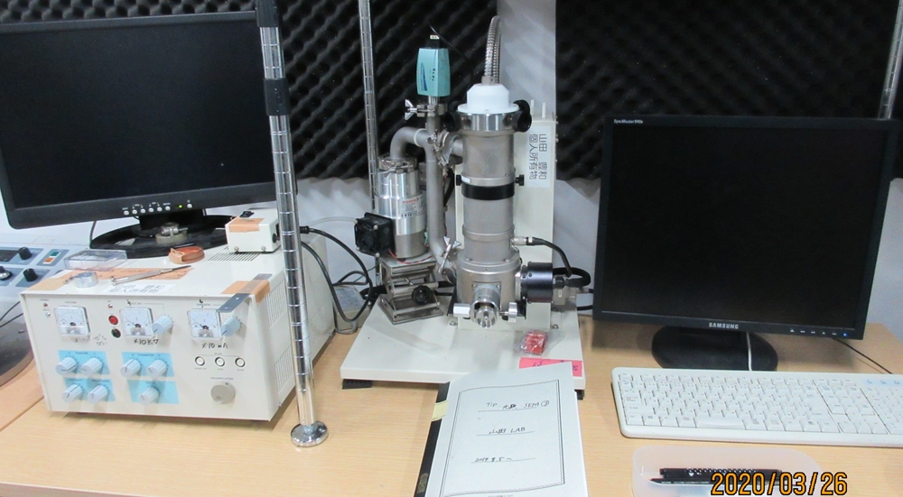
「探針作製装置」自作・化学エッチングとOmicron装置
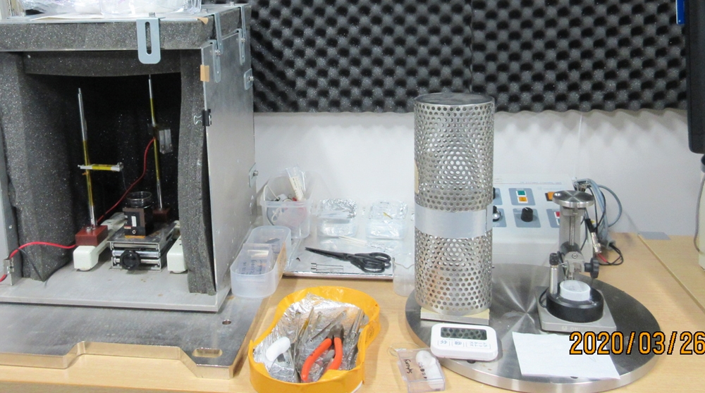
「磁区観察顕微鏡」自作装置
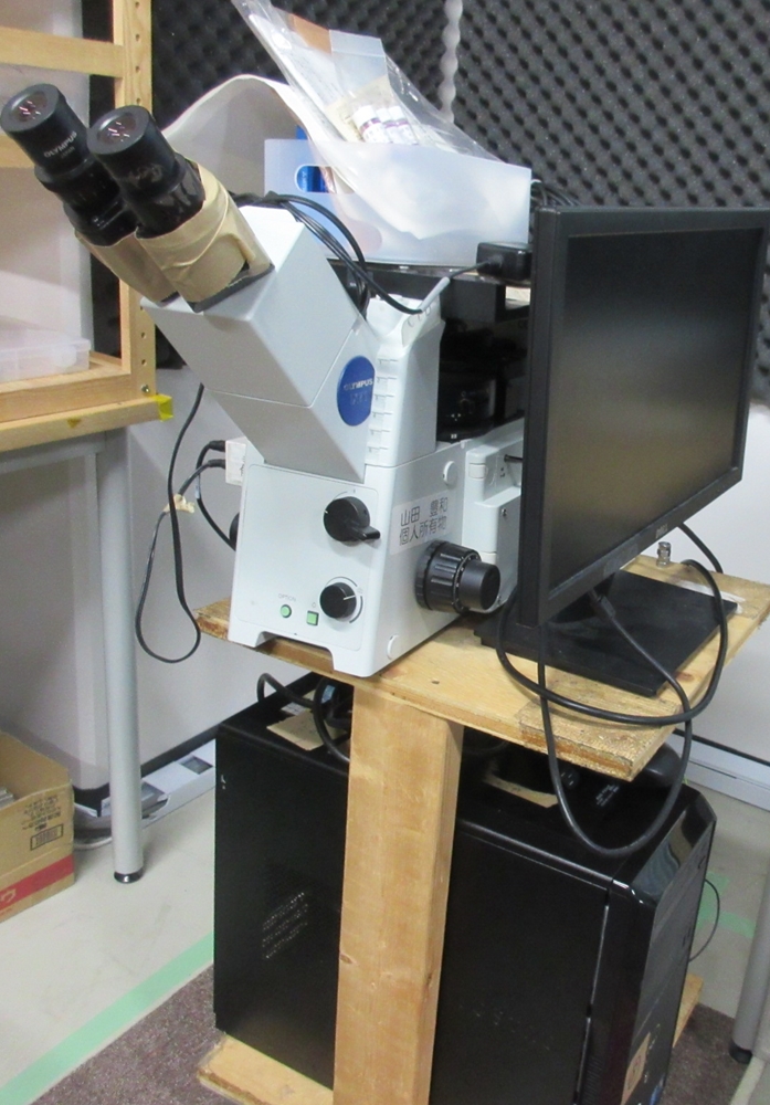
「電気炉」自作・分子昇華精製・CVD用
「VSM」振動試料型磁力計・東英工業社
「探針作製装置」自作・炎エッチング装置
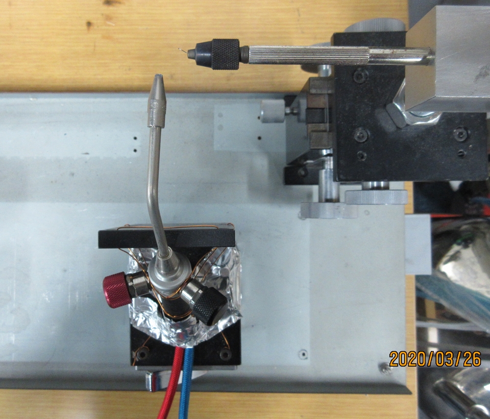
日本学術振興会・人材育成企画委員、
応用物理学会・薄膜表面物理分科会・常任庶務幹事、
日本物理学会・領域9運営委員、
日本磁気学会・講演大会事務局長、
6th Spin-Polarized Scanning Tunneling Microscopy (SP-STM6) conference・Conference Chair、
Program Committee Member of ICSPM and IVC、
他多数歴任。 詳細はこちら。
山田の住居遍歴
兵庫県川西市生まれ(0-2歳)、兵庫県神戸市(2-3歳)、バングラデシュ・ダッカ(3-5歳)、東京都荒川区(5-8歳)、東京都多摩市(8-12歳)、神奈川県平塚市⇔東京目白学習院:往復4時間通学(12-23歳)、オランダ・ナイメーヘン(23-27歳)、東京都豊島区(27-32歳)、ドイツ・カールスルーエ(32-34歳)、千葉県千葉市(34-38歳)、千葉県市原市ちはら台(38歳-41歳)、千葉県船橋市(41歳-)
山田の趣味遍歴
野球->自転車->ジョギング->テニス・ジョギング
2.原子間力顕微鏡(AFM)
3.磁気工学/スピントロニクス
4.分子エレクトロニクス
5.グラフェン技術
6.電子顕微鏡技術
7.電界放出電子顕微鏡
8.表面科学(ナノサイエンス)
9.真空工学
10.低温工学
11.超電導技術
12.結晶工学
13.CAD設計能力
14.画像解析能力
15.プレゼン能力
16.論文執筆能力
17.コミュニケーション能力
18.English能力
1. 表面物理科学(T4-5、木曜日4時限目、工17-211)
2. 力学基礎2(T4-5、木曜日2時限目、工17-214)
3. 力学基礎演習2(T4-5、隔週、水曜日5時限目、17-213)
4. 物質科学基礎演習(1年生担任、T4、木曜日3時限目)
5. 工学入門A(1年生担任、T2、月曜日4時限目)
6. 工学入門B(1年生担任、T4、月曜日4時限目)
7. 工学入門C(1年生担任、T4、水曜日1時限目)
8. 卒業研究
9. 物質科学演習I
10. 物質科学演習II
11. 物質科学実験ⅡA(3年次生)(T1-2、水曜日3-5時限目、6回)
12. 物質科学実験ⅢA(3年次生)(T4-5、水曜日3-5時限目、6回)
13. 物質科学基礎実験A(2年次生)(T1-2、金曜日3-5時限目、2回)
14. 物質科学実験IA(2年次生)(T4-5、金曜日3-5時限目、6回)
大学院
15. 磁性物質科学特論(T1-2、大学院、木曜日5時限目、工17-211)
16. 特別演習Ⅰ(通期、大学院研究ゼミ)
17. 特別研究Ⅰ(通期、大学院研究)
18. 特別演習Ⅱ(通期、大学院研究ゼミ)
19. 特別研究Ⅱ(通期、大学院研究)